mohan-bee/soil-moisture-sensor
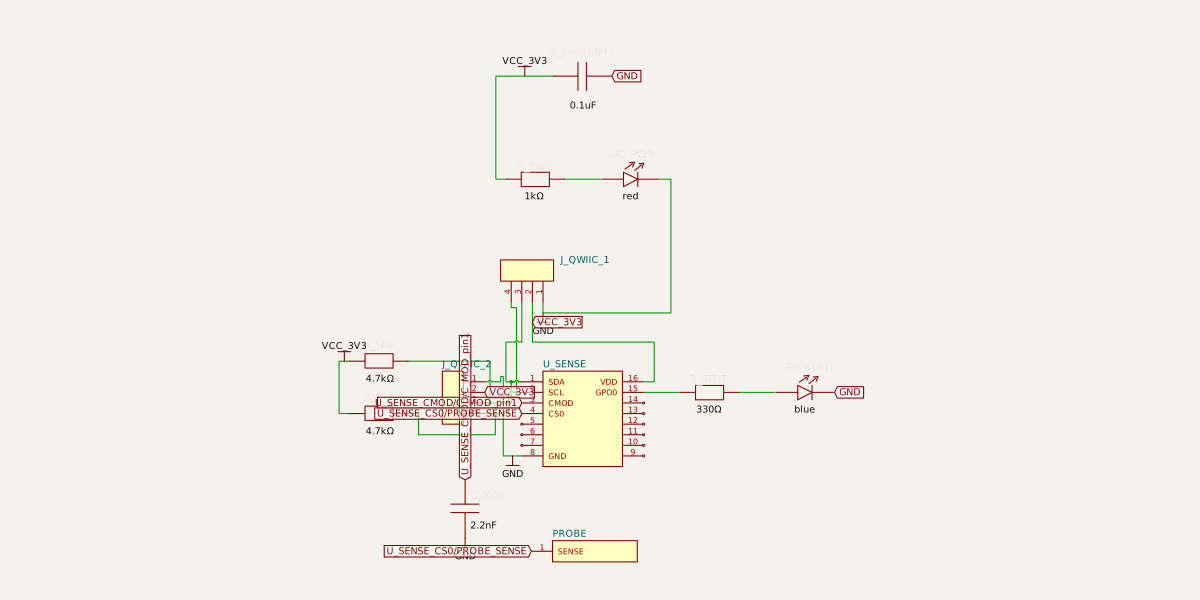
This code defines a compact electronic sensing module featuring a PIC microcontroller, multiple sensors and components, power and status LEDs, and a uniquely designed capacitive soil probe with layered rectangular pads.
- Version
- 0.0.1
- License
- unset
- Stars
- 0
index.tsx
PCB
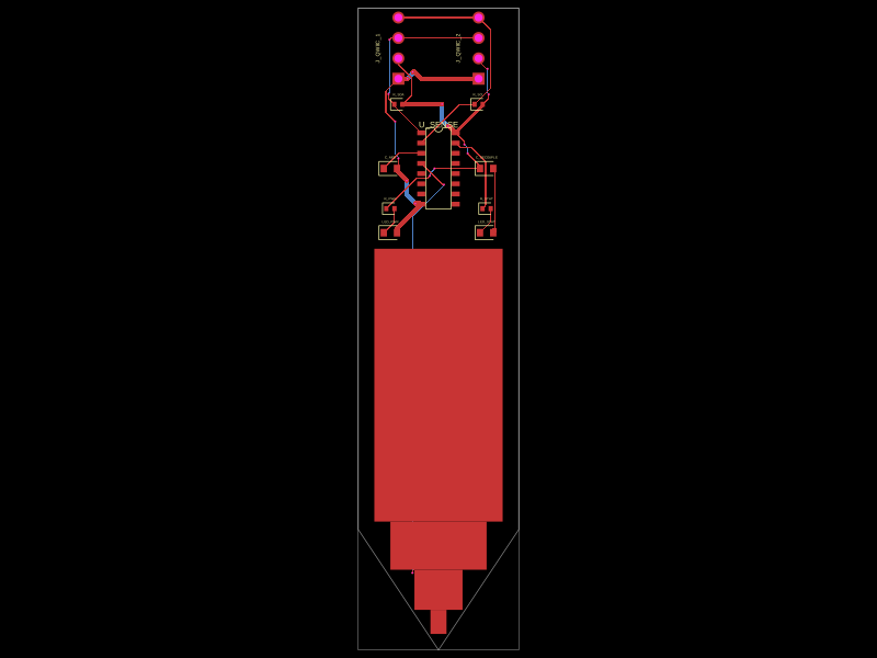
Schematic
import React from "react"

export default () => (
  <board
    width="20mm"
    height="80mm"
    outline={[
      { x: -10, y: 40 },
      { x: 10, y: 40 },
      { x: 10, y: -25 },
      { x: 0, y: -40 },   /* The Pointed Tip */
      { x: -10, y: -25 },
    ]}
  >

    {/* 1. GLOBAL NETS */}
    <net name="VCC_3V3" isPowerNet={true} />
    <net name="GND" isGroundNet={true} />

    {/* ==========================================
        2. COMPONENT PLACEMENT
    ========================================== */}

    <pinheader name="J_QWIIC_1" pinCount={4} pcbX={-5} pcbY={35} pcbRotation={90} />
    <pinheader name="J_QWIIC_2" pinCount={4} pcbX={5} pcbY={35} pcbRotation={90} />

    <chip
      name="U_SENSE"
      footprint="soic16"
      pcbX={0}
      pcbY={20}
      pinLabels={{
        pin1: "SDA", pin2: "SCL", pin3: "CMOD", pin4: "CS0",
        pin8: "GND", pin15: "GPO0", pin16: "VDD"
      }}
    />

    <capacitor name="C_MOD" capacitance="2.2nF" footprint="0603" pcbX={-6} pcbY={20} />
    <capacitor name="C_DECOUPLE" capacitance="0.1uF" footprint="0603" pcbX={6} pcbY={20} />

    <resistor name="R_SDA" resistance="4.7k" footprint="0402" pcbX={-5} pcbY={28} />
    <resistor name="R_SCL" resistance="4.7k" footprint="0402" pcbX={5} pcbY={28} />

    <led name="LED_PWR" color="red" footprint="0603" pcbX={-6} pcbY={12} />
    <resistor name="R_PWR" resistance="1k" footprint="0402" pcbX={-6} pcbY={15} />

    <led name="LED_STAT" color="blue" footprint="0603" pcbX={6} pcbY={12} />
    <resistor name="R_STAT" resistance="330" footprint="0402" pcbX={6} pcbY={15} />

    {/* ==========================================
        ✅ THE FIXED CAPACITIVE SOIL PROBE
        By stacking 4 rectangular pads of decreasing widths,
        we perfectly fill the angled tip without clipping the edge!
    ========================================== */}
    <chip
      name="PROBE"
      pcbX={0}
      pcbY={0}
      pinLabels={{ pin1: "SENSE" }}
      footprint={
        <footprint>
          {/* Main Body (Y=10 to Y=-24) */}
          <smtpad portHints={["pin1"]} pcbX="0mm" pcbY="-7mm" width="16mm" height="34mm" shape="rect" layer="top" />

          {/* Taper Step 1 (Y=-24 to Y=-30) */}
          <smtpad portHints={["pin1"]} pcbX="0mm" pcbY="-27mm" width="12mm" height="6mm" shape="rect" layer="top" />

          {/* Taper Step 2 (Y=-30 to Y=-35) */}
          <smtpad portHints={["pin1"]} pcbX="0mm" pcbY="-32.5mm" width="6mm" height="5mm" shape="rect" layer="top" />

          {/* The Tip (Y=-35 to Y=-38) */}
          <smtpad portHints={["pin1"]} pcbX="0mm" pcbY="-36.5mm" width="2mm" height="3mm" shape="rect" layer="top" />
        </footprint>
      }
    />


    {/* ==========================================
        3. THE ROUTING
    ========================================== */}

    <trace from=".J_QWIIC_1 > .pin1" to="net.GND" thickness="0.6mm" />
    <trace from=".J_QWIIC_1 > .pin2" to="net.VCC_3V3" thickness="0.6mm" />
    <trace from=".J_QWIIC_2 > .pin1" to="net.GND" thickness="0.6mm" />
    <trace from=".J_QWIIC_2 > .pin2" to="net.VCC_3V3" thickness="0.6mm" />

    <trace from=".U_SENSE > .VDD" to="net.VCC_3V3" thickness="0.4mm" />
    <trace from=".U_SENSE > .GND" to="net.GND" thickness="0.4mm" />

    <trace from=".C_DECOUPLE > .pin1" to="net.VCC_3V3" />
    <trace from=".C_DECOUPLE > .pin2" to="net.GND" />

    <trace from=".J_QWIIC_1 > .pin3" to=".J_QWIIC_2 > .pin3" />
    <trace from=".J_QWIIC_1 > .pin4" to=".J_QWIIC_2 > .pin4" />
    <trace from=".J_QWIIC_1 > .pin3" to=".U_SENSE > .SDA" />
    <trace from=".J_QWIIC_1 > .pin4" to=".U_SENSE > .SCL" />

    <trace from=".U_SENSE > .SDA" to=".R_SDA > .pin1" />
    <trace from=".R_SDA > .pin2" to="net.VCC_3V3" />
    <trace from=".U_SENSE > .SCL" to=".R_SCL > .pin1" />
    <trace from=".R_SCL > .pin2" to="net.VCC_3V3" />

    <trace from="net.VCC_3V3" to=".R_PWR > .pin1" />
    <trace from=".R_PWR > .pin2" to=".LED_PWR > .pos" />
    <trace from=".LED_PWR > .neg" to="net.GND" />

    <trace from=".U_SENSE > .GPO0" to=".R_STAT > .pin1" />
    <trace from=".R_STAT > .pin2" to=".LED_STAT > .pos" />
    <trace from=".LED_STAT > .neg" to="net.GND" />

    <trace from=".U_SENSE > .CMOD" to=".C_MOD > .pin1" />
    <trace from=".C_MOD > .pin2" to="net.GND" />

    <trace from=".U_SENSE > .CS0" to=".PROBE > .SENSE" thickness="0.8mm" />

  </board>
)