krishnax12/rs485-breakout
The code models a SparkFun RS-485 transceiver breakout hardware with connected microchip, connectors, resistors, LEDs, capacitors, and mounting holes for serial communication interfacing.
- Version
- 0.1.0
- License
- CC-BY-SA-4.0
- Stars
- 1
index.circuit.tsx
PCB

Schematic
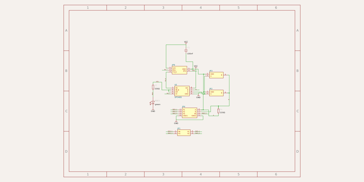
/**
 * SparkFun Transceiver RS-485 Breakout (BOB-10124)
 *
 * Source: https://github.com/sparkfun/RS-485_Breakout
 * Pinned source commit: 08f1d60e6739cf89f001febbcf19147ea7988cf7
 * License: CC BY-SA 4.0
 */

const Sp3485 = () => (
	<chip
		name="U2"
		manufacturerPartNumber="SP3485"
		footprint="soic8"
		pcbX={-3.81}
		pcbY={0}
		schX={0}
		schY={0}
		pinLabels={{
			pin1: "RO",
			pin2: "RE_N",
			pin3: "DE",
			pin4: "DI",
			pin5: "GND",
			pin6: "A",
			pin7: "B",
			pin8: "VCC",
		}}
		pinAttributes={{
			VCC: { requiresPower: true },
			GND: { requiresGround: true },
		}}
		schPinArrangement={{
			leftSide: {
				pins: ["RO", "RE_N", "DE", "DI"],
				direction: "top-to-bottom",
			},
			rightSide: {
				pins: ["VCC", "B", "A", "GND"],
				direction: "top-to-bottom",
			},
		}}
	/>
);

export const SparkFunRs485Breakout = () => (
	<board width="22.86mm" height="27.94mm" routingDisabled>
		<schematicsheet sheetWidth="220mm" sheetHeight="160mm">
			<net name="VCC" isPowerNet />
			<net name="GND" isGroundNet />
			<net name="RTS" />
			{/* Selector-safe equivalents of Eagle's RX-I, TX-O, 1, 2, 3, and 5. */}
			<net name="RX_I" />
			<net name="TX_O" />
			<net name="A" />
			<net name="B" />
			<net name="RJ45_1" />
			<net name="RJ45_2" />
			<net name="RJ45_3" />
			<net name="RJ45_5" />

			<Sp3485 />

			<connector
				name="JP9"
				footprint="pinrow5_p2.54"
				pcbX={-8.89}
				pcbY={5.08}
				schX={-6.8}
				schY={1}
				pinLabels={{
					pin1: "VCC",
					pin2: "RX_I",
					pin3: "TX_O",
					pin4: "RTS",
					pin5: "GND",
				}}
			/>

			<connector
				name="JP2"
				footprint="pinrow3_p3.5"
				pcbX={6.35}
				pcbY={-3.429}
				schX={7.1}
				schY={1.78}
				pinLabels={{ pin1: "GND", pin2: "A", pin3: "B" }}
			/>

			<connector
				name="JP3"
				footprint="pinrow3_p2.54"
				pcbX={10.16}
				pcbY={-2.54}
				schX={7.1}
				schY={0}
				pinLabels={{ pin1: "GND", pin2: "A", pin3: "B" }}
			/>

			<connector
				name="JP4"
				footprint="pinrow8_p2.54"
				pcbX={8.89}
				pcbY={0}
				schX={7.37}
				schY={-2.79}
				pinLabels={{
					pin1: "P1",
					pin2: "P2",
					pin3: "P3",
					pin4: "GND1",
					pin5: "GND2",
					pin6: "P6",
					pin7: "B",
					pin8: "A",
				}}
			/>

			<connector
				name="JP1"
				footprint="pinrow4_p2.54"
				pcbX={-3.81}
				pcbY={-12.7}
				schX={7.37}
				schY={3.81}
				pinLabels={{ pin1: "P6", pin2: "P3", pin3: "P2", pin4: "P1" }}
			/>

			<resistor
				name="R4"
				resistance="220ohm"
				footprint="0603"
				pcbX={-4.064}
				pcbY={5.08}
				schX={9.4}
				schY={1.78}
				schRotation={90}
			/>
			<resistor
				name="R3"
				resistance="330ohm"
				footprint="0603"
				pcbX={-3.81}
				pcbY={-6.35}
				schX={-5.08}
				schY={0}
				schRotation={90}
			/>
			<led
				name="LED3"
				color="green"
				footprint="0603"
				pcbX={-3.81}
				pcbY={-7.874}
				schX={-5.08}
				schY={-1}
				schRotation={90}
			/>
			<capacitor
				name="C3"
				capacitance="100nF"
				footprint="0603"
				pcbX={-6.477}
				pcbY={5.461}
				schX={2.8}
				schY={-0.25}
				schRotation={90}
			/>

			<hole name="H1" diameter="3.2mm" pcbX={-8.89} pcbY={11.43} />
			<hole name="H2" diameter="3.2mm" pcbX={-8.89} pcbY={-11.43} />
			<hole name="H3" diameter="3.2mm" pcbX={8.89} pcbY={11.43} />
			<hole name="H4" diameter="3.2mm" pcbX={8.89} pcbY={-11.43} />

			<trace from=".U2 > .VCC" to="net.VCC" />
			<trace from=".JP9 > .VCC" to="net.VCC" />
			<trace from=".C3 > .pin1" to="net.VCC" />

			<trace from=".U2 > .GND" to="net.GND" />
			<trace from=".JP9 > .GND" to="net.GND" />
			<trace from=".JP2 > .GND" to="net.GND" />
			<trace from=".JP3 > .GND" to="net.GND" />
			<trace from=".JP4 > .GND1" to="net.GND" />
			<trace from=".JP4 > .GND2" to="net.GND" />
			<trace from=".C3 > .pin2" to="net.GND" />
			<trace from=".LED3 > .cathode" to="net.GND" />

			<trace from=".U2 > .RE_N" to="net.RTS" />
			<trace from=".U2 > .DE" to="net.RTS" />
			<trace from=".JP9 > .RTS" to="net.RTS" />
			<trace from=".R3 > .pin2" to="net.RTS" />
			<trace name="N$4" from=".R3 > .pin1" to=".LED3 > .anode" />

			<trace from=".U2 > .DI" to="net.RX_I" />
			<trace from=".JP9 > .RX_I" to="net.RX_I" />
			<trace from=".U2 > .RO" to="net.TX_O" />
			<trace from=".JP9 > .TX_O" to="net.TX_O" />

			<trace from=".U2 > .A" to="net.A" />
			<trace from=".JP2 > .A" to="net.A" />
			<trace from=".JP3 > .A" to="net.A" />
			<trace from=".JP4 > .A" to="net.A" />
			<trace from=".R4 > .pin1" to="net.A" />

			<trace from=".U2 > .B" to="net.B" />
			<trace from=".JP2 > .B" to="net.B" />
			<trace from=".JP3 > .B" to="net.B" />
			<trace from=".JP4 > .B" to="net.B" />
			<trace from=".R4 > .pin2" to="net.B" />

			<trace from=".JP4 > .P1" to="net.RJ45_1" />
			<trace from=".JP1 > .P1" to="net.RJ45_1" />
			<trace from=".JP4 > .P2" to="net.RJ45_2" />
			<trace from=".JP1 > .P2" to="net.RJ45_2" />
			<trace from=".JP4 > .P3" to="net.RJ45_3" />
			<trace from=".JP1 > .P3" to="net.RJ45_3" />
			<trace from=".JP4 > .P6" to="net.RJ45_5" />
			<trace from=".JP1 > .P6" to="net.RJ45_5" />
		</schematicsheet>
	</board>
);

export default SparkFunRs485Breakout;
Related Packages
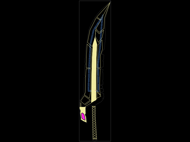 More from this authorkrishnax12/tensa-zangetsu-keychain-nfcThis code defines a PCB footprint and 3D model for an NFC-enabled electronic component featuring an NXP NT2H1311F0DTLH chip, a PCB copper coil antenna, and a custom-shaped, silkscreen-illustrated metal blade housing.
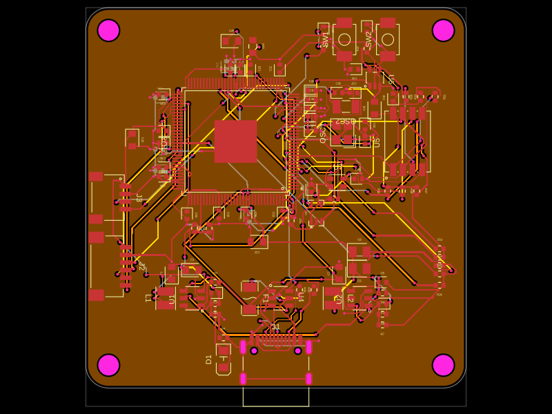 Similar packagetechmannih/trellis-coreThis code defines a detailed electronic hardware system including various surface-mount components such as connectors, voltage regulators, capacitors, resistors, LEDs, microcontroller chips, and modules, all with associated physical footprints, 3D models, and circuit connectivity.
 Discover something newShiboSoftwareDev/mspm0g3507-usb-c-dev-boardThe circuit assembles a USB-C port with integrated ESD protection, power regulation, UART interface, and microcontroller (MSPM0G3507) with supporting components for USB data lines, CC termination, I2C, SPI, reset circuitry, and indicator LEDs.