imrishabh18/test-pcm
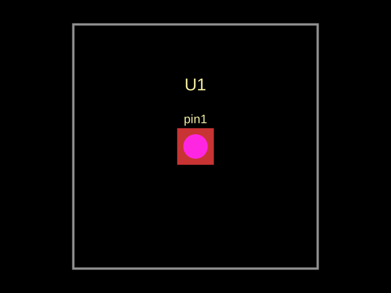
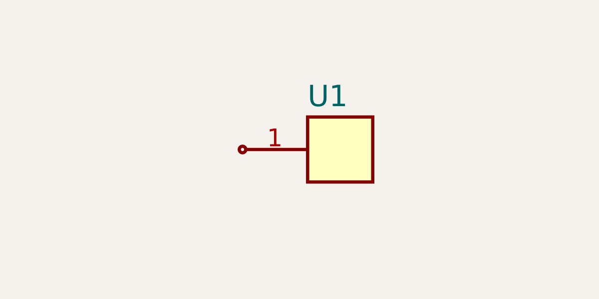
This code defines a 10mm by 10mm electronic circuit board containing a single pin-row chip with an associated 3D CAD model of the "MachineContactMedium" component.
- Version
- 1.0.3
- License
- unset
- Stars
- 0
dist/pcb.svg
PCB
Schematic
<svg xmlns="http://www.w3.org/2000/svg" width="800" height="600" data-software-used-string="@tscircuit/core@0.0.980"><style></style><rect class="boundary" x="0" y="0" fill="#000" width="800" height="600" data-type="pcb_background" data-pcb-layer="global"/><rect class="pcb-boundary" fill="none" stroke="#fff" stroke-width="0.3" x="150" y="50" width="500" height="500" data-type="pcb_boundary" data-pcb-layer="global"/><path class="pcb-board" d="M 150 550 L 650 550 L 650 50 L 150 50 Z" fill="none" stroke="rgba(255, 255, 255, 0.5)" stroke-width="5" data-type="pcb_board" data-pcb-layer="board"/><text x="0" y="0" dx="0" dy="0" fill="#f2eda1" font-family="Arial, sans-serif" font-size="25" text-anchor="middle" dominant-baseline="central" transform="matrix(1,0,0,1,400,243.75)" class="pcb-silkscreen-text pcb-silkscreen-top" data-pcb-silkscreen-text-id="pcb_component_0" stroke="none" data-type="pcb_silkscreen_text" data-pcb-layer="top">pin1</text><text x="0" y="0" dx="0" dy="0" fill="#f2eda1" font-family="Arial, sans-serif" font-size="35" text-anchor="middle" dominant-baseline="central" transform="matrix(1,0,0,1,400,173)" class="pcb-silkscreen-text pcb-silkscreen-top" data-pcb-silkscreen-text-id="pcb_component_0" stroke="none" data-type="pcb_silkscreen_text" data-pcb-layer="top">U1</text><g data-type="pcb_plated_hole" data-pcb-layer="through"><rect class="pcb-hole-outer-pad" fill="rgb(200, 52, 52)" x="362.5" y="262.5" width="75" height="75" data-type="pcb_plated_hole" data-pcb-layer="top"/><circle class="pcb-hole-inner" fill="#FF26E2" cx="400" cy="300" r="25" data-type="pcb_plated_hole_drill" data-pcb-layer="drill"/></g></svg>Related Packages
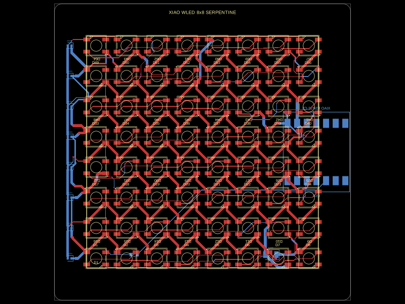 More from this authorimrishabh18/desk-led-matrixThis code models a hardware setup comprising a WLED-compatible LED cascade array connected to a XIAO ESP32-C3 microcontroller, including power regulation components and detailed PCB layout with traces, pads, and silkscreen markings.
 Similar packageMustafaMulla29/wireless-mouse-pcbThis code defines a 3.3V low dropout voltage regulator chip (AP2112K-3.3TRG1) with five pins (VIN, GND, Enable, NC, VOUT) and its associated PCB footprint and 3D models for hardware implementation.
 Discover something newhrithik18k/smart-switch-pcbThe AO3400A component models a SOT-23 N-channel MOSFET with labeled pins for Gate, Source, and Drain, including 3D CAD models and schematic symbols for electronic circuit design.