imrishabh18/rp2040-motor-controller
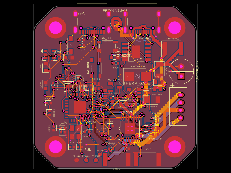
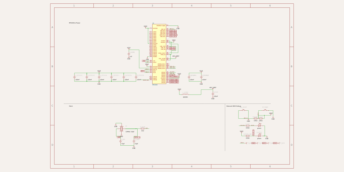
This circuit module provides a microcontroller-based NEMA17 stepper motor driver with integrated USB-C Power Delivery, temperature sensing, and safety interlocks.
- Version
- 1.0.16
- License
- unset
- Stars
- 0
index.circuit.tsx
PCB
Schematic
import nema17Outline from "./mechanical/nema17-outline.json";
import { savedRouting } from "./routing/saved-routing";
import { ControllerSections } from "./schematic/ControllerSections";
import {
	MotorDriverController,
	MotorDriverControlTraces,
	MotorDriverGroundTraces,
	MotorDriverPassives,
	MotorDriverPowerTraces,
	MotorDriverPrimaryGroundTraces,
	MotorDriverSenseAndControlTraces,
} from "./schematic/MotorDriverCoreSection";
import {
	MotorOutputConnectors,
	MotorOutputTraces,
} from "./schematic/MotorOutputsSection";
import {
	MotorPowerFilteringComponents,
	MotorPowerFilteringGroundTrace,
	MotorPowerFilteringSupplyTrace,
} from "./schematic/MotorPowerFilteringSection";
import {
	MotorPowerPdConnectorGroundTraces,
	MotorPowerPdControllers,
	MotorPowerPdInputTraces,
	MotorPowerPdPassives,
	MotorPowerPdPrimaryGroundTrace,
	MotorPowerPdProtocolTraces,
	MotorPowerPdSupportGroundTraces,
} from "./schematic/MotorPowerPdNegotiationSection";
import { SchematicSheets } from "./schematic/SchematicSheets";
import { ThermalProtectionComponents, ThermalProtectionTraces } from "./schematic/ThermalProtectionSection";

export default function Rp2040MotorController({
	routingDisabled = false,
}: {
	routingDisabled?: boolean;
} = {}) {
	return (
    <board
      routingDisabled={routingDisabled}
			layers={4}
      thickness="1.6mm"
			outline={nema17Outline}
			minViaHoleDiameter="0.3mm"
      minViaPadDiameter="0.45mm"
			autorouterEffortLevel="2x"
			autorouterVersion="beta_pipeline7"
			autorouter={{
				local: true,
				algorithmFn: savedRouting,
				groupMode: "subcircuit",
			}}
		>
			<net name="GND" />
			{/* Explicit net names keep labels consistent across the MCU subcircuit and sheets. */}
			<net name="DRIVER_AIN1" connectsTo=".MCU > .U1 > .GPIO18" />
			<net name="DRIVER_AIN2" connectsTo=".MCU > .U1 > .GPIO19" />
			<net name="DRIVER_BIN1" connectsTo=".MCU > .U1 > .GPIO20" />
			<net name="MCU_ENABLE" connectsTo=".MCU > .U1 > .GPIO22" />
			<net name="TEMP_OK" connectsTo=".MCU > .U1 > .GPIO24" />
			<net name="TEMP_SDA" connectsTo=".MCU > .U1 > .GPIO26_ADC0" />
			<net name="TEMP_SCL" connectsTo=".MCU > .U1 > .GPIO27_ADC1" />
			<SchematicSheets />

			<group pcbX={-5.625} pcbY={-8.25}>
				<ControllerSections />
				<MotorDriverController />
				<MotorPowerPdControllers />
				<MotorOutputConnectors />
				<MotorPowerFilteringComponents />
				<MotorPowerPdPassives />
				<MotorDriverPassives />
				<ThermalProtectionComponents />

				<MotorDriverControlTraces />
				<MotorPowerPdInputTraces />
				<MotorPowerFilteringSupplyTrace />
				<MotorPowerPdProtocolTraces />
				<MotorDriverPowerTraces />
				<MotorDriverPrimaryGroundTraces />
				<MotorPowerPdPrimaryGroundTrace />
				<MotorPowerPdConnectorGroundTraces />
				<MotorPowerFilteringGroundTrace />
				<MotorPowerPdSupportGroundTraces />
				<MotorDriverGroundTraces />
				<MotorOutputTraces />
				<MotorDriverSenseAndControlTraces />
				<ThermalProtectionTraces />
			</group>

			<copperpour
				name="GND_TOP"
				layer="top"
				connectsTo="net.GND"
				clearance="0.2mm"
				padMargin="0.2mm"
				traceMargin="0.2mm"
				boardEdgeMargin="0.3mm"
				coveredWithSolderMask
			/>
			<copperpour
				name="GND_BOTTOM"
				layer="bottom"
				connectsTo="net.GND"
				clearance="0.2mm"
				padMargin="0.2mm"
				traceMargin="0.2mm"
				boardEdgeMargin="0.3mm"
				coveredWithSolderMask
			/>

			<group pcbX={0} pcbY={0} schX={0} schY={0}>
        {[-15.5,15.5].flatMap(x => [-15.5,15.5].map(y => (
          <group key={`${x}:${y}`} pcbX={0} pcbY={0} schX={0} schY={0}>
            <chip name={`MH${(x > 0 ? 2 : 0) + (y > 0 ? 1 : 0) + 1}`} pcbX={x} pcbY={y} schSheetName="motor_power" schX={x > 0 ? 10 : 7} schY={y > 0 ? -4 : -6}
              pinLabels={{pin1:["GND"]}} connections={{pin1:"net.GND"}}
              footprint={<footprint><platedhole portHints={["pin1"]} shape="circle" holeDiameter="3.3mm" outerDiameter="5.6mm" /></footprint>} />
          </group>
        )))}
        <silkscreentext text="RP2040 NEMA17" pcbX={0} pcbY={20} fontSize="0.8mm" />
      </group>
			{/* Explicit source joins also give the MCU sheet the same net labels. */}
			<trace name="LABEL_AIN1" from=".MCU > .U1 > .GPIO18" to="net.DRIVER_AIN1" schDisplayLabel="DRIVER_AIN1" />
			<trace name="LABEL_AIN2" from=".MCU > .U1 > .GPIO19" to="net.DRIVER_AIN2" schDisplayLabel="DRIVER_AIN2" />
			<trace name="LABEL_BIN1" from=".MCU > .U1 > .GPIO20" to="net.DRIVER_BIN1" schDisplayLabel="DRIVER_BIN1" />
			<trace name="LABEL_ENABLE" from=".MCU > .U1 > .GPIO22" to="net.MCU_ENABLE" schDisplayLabel="MCU_ENABLE" />
			<trace name="LABEL_TEMP_OK" from=".MCU > .U1 > .GPIO24" to="net.TEMP_OK" schDisplayLabel="TEMP_OK" />
			<trace name="LABEL_TEMP_SDA" from=".MCU > .U1 > .GPIO26_ADC0" to="net.TEMP_SDA" schDisplayLabel="TEMP_SDA" />
			<trace name="LABEL_TEMP_SCL" from=".MCU > .U1 > .GPIO27_ADC1" to="net.TEMP_SCL" schDisplayLabel="TEMP_SCL" />
		</board>
	);
}
Related Packages
 More from this authorimrishabh18/untitled-package-69Creates a 10mm × 10mm PCB with a 1kΩ resistor and a 1000pF capacitor connected in series.
 Similar packageaura/diy-power-delivery-triggerThis hardware design implements a USB Type-C port with supporting power management and signal conditioning components, including a USB-C connector, a FUSB302 USB-C port controller, ESD protection diodes, a buck converter for 3.3V power regulation, an STM32 microcontroller for control and processing, an RGB LED indicator, push button, terminal block connections, and associated filtering and support components.
 Discover something newShiboSoftwareDev/mspm0g3507-usb-c-dev-boardThe circuit assembles a USB-C port with integrated ESD protection, power regulation, UART interface, and microcontroller (MSPM0G3507) with supporting components for USB data lines, CC termination, I2C, SPI, reset circuitry, and indicator LEDs.