imrishabh18/pedometer
This code defines and assembles a simple radio receiver hardware circuit using specific imported capacitors, inductors, RF connectors, and oscillator components with precise footprints and schematic attributes.
- Version
- 1.1.3
- License
- unset
- Stars
- 0
tests/manufacturing.test.ts
import { expect, test } from "bun:test"
import { readFileSync } from "node:fs"
import type { AnyCircuitElement } from "circuit-json"
import { prepareManufacturingCircuit } from "../manufacturing"
import { convertCircuitJsonToGerberFiles } from "circuit-json-to-gerber"
import { pointToSegmentDistance } from "@tscircuit/math-utils"

const input: AnyCircuitElement[] = JSON.parse(readFileSync("dist/index/circuit.json", "utf8"))
const output = prepareManufacturingCircuit(input)

test("manufacturing preparation preserves copper, nets, and generated drills", () => {
  const withoutPasteOrMask = (c: AnyCircuitElement[]) => c.filter(e => e.type !== "pcb_solder_paste" && !e.type.startsWith("pcb_silkscreen_")).map(e => {
    if (e.type !== "pcb_smtpad") return e
    const { soldermask_margin, ...rest } = e
    return rest
  })
  expect(withoutPasteOrMask(output)).toEqual(withoutPasteOrMask(input))
  expect(prepareManufacturingCircuit(output)).toEqual(output)
})

test("fabrication legend uses the clear underside and printable text strokes", () => {
  const silk=output.filter(e=>e.type.startsWith("pcb_silkscreen_"))
  expect(silk).toHaveLength(4)
  for(const e of silk){
    if(e.type!=="pcb_silkscreen_text")throw new Error("Unexpected fabrication silk")
    expect(e.layer).toBe("bottom")
    expect(e.font_size*0.09).toBeGreaterThanOrEqual(0.15)
  }
})

test("29 TI stencil openings have the rounded-square outline and area", () => {
  const paste = output.filter(e => e.type === "pcb_solder_paste" && /^pcb_smtpad_.*_paste_/.test(e.pcb_solder_paste_id))
  const padIds = new Set(paste.map(e => e.type === "pcb_solder_paste" ? e.pcb_smtpad_id : ""))
  expect(padIds.size).toBe(29)
  for (const id of padIds) {
    const parts = paste.filter(e => e.type === "pcb_solder_paste" && e.pcb_smtpad_id === id)
    expect(parts).toHaveLength(6)
  }
  const parts = paste.filter(e => e.type === "pcb_solder_paste" && e.pcb_smtpad_id === [...padIds][0])
  const pad = output.find(e => e.type === "pcb_smtpad" && e.pcb_smtpad_id === [...padIds][0])!
  if (pad.type !== "pcb_smtpad" || pad.shape !== "circle") throw new Error("Missing BGA land")
  let occupied = 0
  const n = 400, step = 0.3 / n
  for (let i = 0; i < n; i++) for (let j = 0; j < n; j++) {
    const x = pad.x - 0.15 + (i + 0.5) * step, y = pad.y - 0.15 + (j + 0.5) * step
    if (parts.some(e => e.type === "pcb_solder_paste" && (e.shape === "circle"
      ? Math.hypot(x - e.x, y - e.y) <= e.radius
      : e.shape === "rect" && Math.abs(x - e.x) <= e.width / 2 && Math.abs(y - e.y) <= e.height / 2))) occupied++
  }
  expect(Math.abs(occupied * step ** 2 - (0.25 ** 2 - (4 - Math.PI) * 0.05 ** 2))).toBeLessThan(0.0002)
})

test("installed exporter emits each through-via and USB shell slot once", () => {
  const files = convertCircuitJsonToGerberFiles(output)
  expect(Object.keys(files).filter(n => n.endsWith(".drl")).sort()).toEqual(["drill-L1-L4.drl", "drill_npth.drl"])
  const holes = files["drill-L1-L4.drl"].match(/^X-?[\d.]+Y-?[\d.]+$/gm) ?? []
  const vias = output.filter(e => e.type === "pcb_via")
  expect(holes.length).toBe(new Set(holes).size)
  const slots = output.filter(e => e.type === "pcb_plated_hole")
  expect(slots).toHaveLength(4)
  expect(files["drill-L1-L4.drl"].match(/^G85/gm)).toHaveLength(4)
  expect(holes.length).toBe(new Set(vias.map(e => e.type === "pcb_via" ? `${e.x.toFixed(4)},${e.y.toFixed(4)}` : "")).size + slots.length)
})

test("QFN exposed pad uses four TI-sized stencil windows instead of full-pad paste", () => {
  const paste=output.filter(e=>e.type==="pcb_solder_paste" && e.pcb_solder_paste_id.startsWith("qfn_ep_window_"));
  expect(paste).toHaveLength(24);
  const pads=new Set(paste.map(e=>e.type==="pcb_solder_paste"?e.pcb_smtpad_id:undefined));
  expect(pads.size).toBe(1);
  const all=output.filter(e=>e.type==="pcb_solder_paste" && pads.has(e.pcb_smtpad_id));
  expect(all).toHaveLength(24);
  const windows=paste.filter(e=>e.type==="pcb_solder_paste"&&e.pcb_solder_paste_id.endsWith("_h"));
  expect(windows).toHaveLength(4);
  for(const w of windows){if(w.type!=="pcb_solder_paste"||w.shape!=="rect")throw new Error("Missing QFN window");expect(w.width).toBe(1.08);expect(w.height).toBeCloseTo(0.98,8);}
})

test("routed through-holes clear other-net traces on every layer", () => {
  const traces = input.filter(e => e.type === "pcb_trace")
  const net = (id: string | undefined) => (traces.find(t => t.pcb_trace_id === id) as any)?.connection_name
  const segments = traces.flatMap(t => t.route.flatMap((a, i) => {
    const b = t.route[i + 1]
    return a.route_type === "wire" && b?.route_type === "wire" && a.layer === b.layer
      ? [{ a, b, net: net(t.pcb_trace_id) }] : []
  }))
  let minimum = Infinity
  for (const via of input.filter(e => e.type === "pcb_via")) {
    expect(via.hole_diameter).toBe(0.15)
    expect(via.outer_diameter).toBe(0.3)
    expect(via.layers).toEqual(["top", "inner1", "inner2", "bottom"])
    const viaNet = net(via.pcb_trace_id)
    expect(viaNet).toBeDefined()
    for (const segment of segments) if (segment.net !== viaNet) {
      minimum = Math.min(minimum, pointToSegmentDistance(via, segment.a, segment.b)
        - via.hole_diameter / 2 - Math.max(segment.a.width, segment.b.width) / 2)
    }
  }
  expect(minimum).toBeGreaterThanOrEqual(0.2)
})
Related Packages
 More from this authorimrishabh18/test-pcmThis code defines a 10mm by 10mm electronic circuit board containing a single pin-row chip with an associated 3D CAD model of the "MachineContactMedium" component.
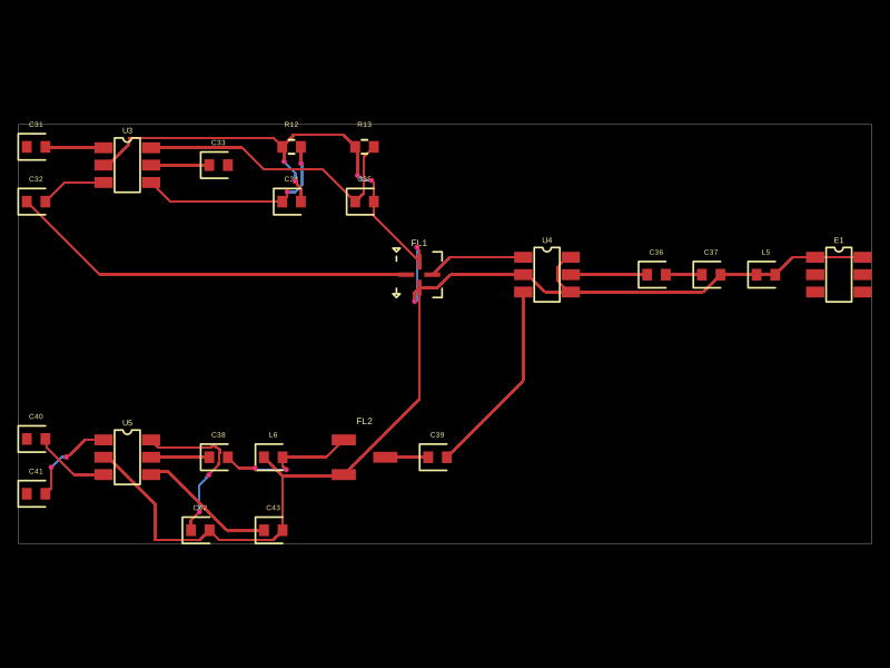 Similar packageMustafaMulla29/CC3235SF-tsxThis code defines a PCB layout with RF front-end components including RF switches (RTC6608OSP), band-pass filters, a diplexer, matching capacitors and inductors, and an antenna, all arranged to match a specific schematic for high-frequency radio signal routing.
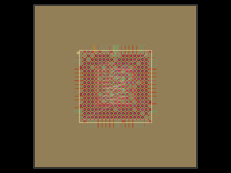 Discover something new0hmX/am3352This code defines a six-layer printed circuit board (PCB) design with a TI AM3352 microprocessor package, including precise pin mapping, power plane definition, fixed component placement, and PCB layout visualization.