imrishabh18/pedometer
This code defines and assembles a simple radio receiver hardware circuit using specific imported capacitors, inductors, RF connectors, and oscillator components with precise footprints and schematic attributes.
- Version
- 1.1.3
- License
- unset
- Stars
- 0
docs/bare-cc2340r5.md
# Bare CC2340R5 revision

The local Rev B design replaces M1/RF-BM-2340C2 with **U1, CC2340R52E0RGER**, a 4 x 4 mm QFN24 with a 2.45 mm exposed ground pad. There is no RF module in the active circuit. The BQ25150, BQ27427, BMA400, USB-C charger input and JST battery/OLED/SWD connectors remain.

The board is **40 × 38 × 1 mm**, enlarged from the prior 34 × 32 mm bare-chip layout to separate component groups and give the autorouter complete routing corridors. USB-C stays aligned to the top edge; ANT1 stays at the upper-left corner.

## Circuit changes

- U1 VDDS pins 11/18/24 use the 2.5 V main supply. C1/C19/C20 provide local 100 nF decoupling, and C2 supplies bulk decoupling.
- The internal DC/DC converter uses L1 (10 uH) from DCDC pin 17 to MCU_VDDR. C21 is the required 10 uF bulk capacitor. Pins 2 and 20 connect to MCU_VDDR with C25/C22 local 100 nF decoupling. This internal rail is not connected to the external 2.5 V supply. Enable DC/DC using the TI power driver; the 2.5 V rail exceeds the 2.2 V enable threshold.
- VDDD pin 16 uses C23 (1 uF) to ground and does not supply external circuitry. Pins 23 and 25 connect to ground.
- Y2 is Abracon ABM11W-48.0000MHZ-8-D1X-T3: 48 MHz, 8 pF load, 40 ohm maximum ESR. It connects to pins 21/22. Configure the internal crystal capacitor array and characterize its frequency offset; the nominal 8 pF load is not a measured board setting. Review the current TI datasheet's caveat about external capacitors for particular regulatory targets before release.
- Y1 retains the 32.768 kHz crystal and initial 12/15 pF loads on pins 14/15. R14/C24 add the reference 100 kohm / 100 nF reset network; J4 retains SWD and reset access.
- C26/L2/C27 implement TI's RF low-pass network: 1.5 pF shunt, 2.8 nH series, 1.5 pF shunt. All three use 0201 packages.
- ANT1 is a separate Johanson 2450AT18A100E ceramic antenna. Pin 1 is the feed; pin 2 is an isolated mechanical solder terminal, not ground. Its 6.5 x 6.5 mm corner region is clear of other copper except the antenna/feed. Keep battery and display metal away from this region.
- C28/L3/L4 provide the Johanson tee tuning network: 1 pF series, 2.7 nH shunt, 3.9 nH series. These are evaluation-board starting values. Tune the assembled board with the enclosure, battery and display fitted.

Physical inner1 is reserved for the ground pour. The autorouter uses top, inner2 and bottom for signal routing. Through-vias and their antipads still cross the ground plane; the antenna keepout removes copper on all layers.

RF and both oscillator nets are routed first on the top layer by the autorouter, with no manually placed vias. The 0.20 mm RF width is a provisional layout value; confirm its impedance against the factory stackup and verify an uninterrupted ground reference before production. The separate chip antenna keeps the board compact; a custom PCB radiator is not required for this implementation.

The QFN lands were checked against TI RGE0024B (0.50 mm pitch, 0.60 × 0.25 mm peripheral lands, 2.45 mm exposed pad). The Y2 import now follows Abracon’s recommended 0.875 × 0.775 mm lands at 1.275 × 0.975 mm center spacing. The antenna lands follow Johanson’s 4.2 mm outer span and 2.6 mm inner gap.

## Firmware pin mapping

GPIO assignments are unchanged. Package numbers change because the module contacts are gone.

| Function | CC2340R5 DIO | U1 QFN pin |
|---|---:|---:|
| I2C SCL | 6 | 19 |
| I2C SDA | 8 | 3 |
| Accelerometer INT1 | 12 | 5 |
| Gauge GPOUT | 21 | 10 |
| PMIC INT | 13 | 6 |
| Button / PMIC PG | 24 | 12 |
| PMIC LP | 11 | 4 |
| Display isolation | 20 | 9 |
| SWDIO | 16 | 7 |
| SWCLK | 17 | 8 |
| LF crystal P / N | 3 / 4 | 14 / 15 |
| Reset | — | 13 |

Select CC2340R52E0RGER in TI SysConfig. The host-tested C core is still not a complete TI target firmware build.

## References and verification scope

- [TI CC2340R5 datasheet, SWRS272F](https://www.ti.com/lit/ds/symlink/cc2340r5.pdf): pin table and RGE0024B package/land pattern.
- [TI RGE LaunchPad reference design, SWRR189A](https://www.ti.com/lit/zip/swrr189): downloaded schematic, BOM and PCB design files.
- [TI hardware design guide, SWRA834A](https://www.ti.com/lit/pdf/swra834): RF, clock, supply and layout guidance.
- [Abracon ABM11W specifications](https://abracon.com/Resonators/ABM11W.pdf).
- [Johanson antenna and mounting requirements](https://www.johansontechnology.com/docs/3827/Antenna-2450AT18A0100001E-Rev4.0.pdf).

Live JLCSearch records for the replacement chip and added purchased components are saved in `review/bare-mcu-stock.json`. RF performance, oscillator calibration, enclosure interaction and assembly process acceptance require physical prototype work. The current CAD and fabrication-package status is recorded in [fabrication review](fabrication-review.md); earlier module-board reviews are historical.
Related Packages
 More from this authorimrishabh18/test-pcmThis code defines a 10mm by 10mm electronic circuit board containing a single pin-row chip with an associated 3D CAD model of the "MachineContactMedium" component.
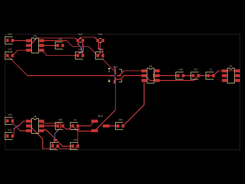 Similar packageMustafaMulla29/CC3235SF-tsxThis code defines a PCB layout with RF front-end components including RF switches (RTC6608OSP), band-pass filters, a diplexer, matching capacitors and inductors, and an antenna, all arranged to match a specific schematic for high-frequency radio signal routing.
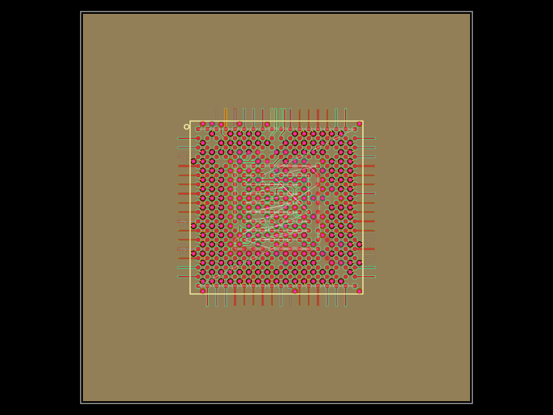 Discover something new0hmX/am3352This code defines a six-layer printed circuit board (PCB) design with a TI AM3352 microprocessor package, including precise pin mapping, power plane definition, fixed component placement, and PCB layout visualization.