imrishabh18/pedometer
This code defines and assembles a simple radio receiver hardware circuit using specific imported capacitors, inductors, RF connectors, and oscillator components with precise footprints and schematic attributes.
- Version
- 1.1.3
- License
- unset
- Stars
- 0
docs/assembly-requirements.md
# Prototype fabrication and assembly requirements

This is the process specification for the CAM review package. Factory acceptance of this revised package has not been obtained. It replaces the passive pad geometry rejected in the previous order.

- Board: 40 × 38 mm, four copper layers, 1.0 mm FR-4, ENIG, green soldermask. Outer copper 1 oz; inner copper 0.5 oz. Confirm the dielectric stackup and RF impedance before tooling.
- Layer order: F_Cu, In1_Cu (ground reference), In2_Cu, B_Cu. All vias span all four layers. No blind or buried vias.
- Through-vias: 0.15 mm drill and 0.30 mm copper diameter. **Resin-fill, planarize and copper-cap all plated vias**, including those in BGA/QFN/passive pads. Do not apply fill to USB-C mounting slots or NPTH mounting holes. Use X-ray inspection for BGA and QFN solder joints.
- U2 via-in-pad lands have 0.23 mm soldermask openings over 0.30 mm annuli, giving nominal 0.035 mm radial mask overlap. Factory CAM must explicitly accept mask registration and the resulting solder-mask-defined joints. Do not expand their openings to expose the full via annulus without a design review. The exact locations are in `review/bga-via-inventory.json`.
- Other BGA lands use 0.025 mm radial NSMD expansion; the aperture audit checks at least 0.10 mm of mask bridge between BGA openings.
- U2/U3 paste: 0.25 mm rounded squares, R0.05, with a nominal 0.10 mm stencil. U1 exposed-pad paste: four 1.08 mm rounded squares, R0.05, at ±0.64 mm, approximately 78% coverage. TI's U1 example uses 0.125 mm stencil thickness; the assembler must approve a common or stepped stencil and paste transfer.
- Supply a handling panel with rails, tooling holes and fiducials appropriate to the assembly line. Only the single-board outline is supplied. Place breakaway tabs away from ANT1 and connector openings; maintain the all-layer antenna keepout.
- Use the included PCB-only BOM and CPL. CPL coordinates share the Gerbers' board-center origin; the board extends from X −20 to +20 and Y −19 to +19 mm. Check imported component pin 1, placement rotations and centers against the assembly drawing before machine setup. Do not infer polarity from cable colors.
- Fabrication silkscreen uses four readable legends on the underside, with 1.7 mm text and 0.153 mm strokes. Dense top-side references remain in the assembly drawing, not the soldering area.
- RF: request a 50 Ω top-layer feed referenced to In1_Cu. The routed width is 0.20 mm and nearby top-ground spacing is geometry-dependent. CAM must confirm a compatible stackup and impedance calculation; return any requested width/clearance change for rerouting and review. Prototype antenna tuning is still required in the final enclosure.

The [TI BQ25150](https://www.ti.com/lit/ds/symlink/bq25150.pdf), [BQ27427](https://www.ti.com/lit/ds/symlink/bq27427.pdf), and [CC2340R5](https://www.ti.com/lit/ds/symlink/cc2340r5.pdf) drawings inform the pad/stencil geometry. [JLCPCB's capabilities](https://jlcpcb.com/capabilities/pcb-capabilities) specify fine-pitch BGA, via filling and drill/clearance constraints. Process acceptance remains separate from passing CAD checks.
Related Packages
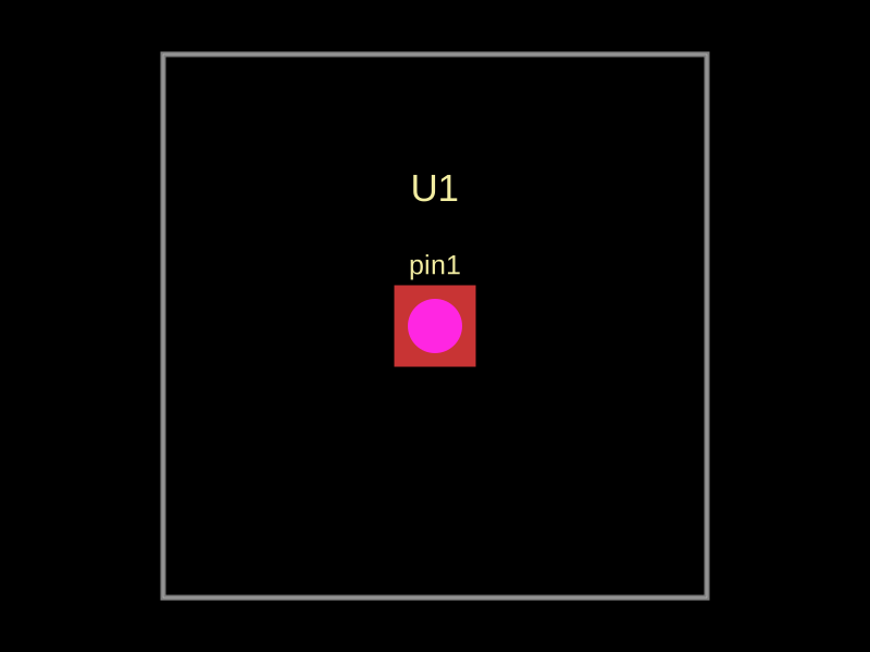 More from this authorimrishabh18/test-pcmThis code defines a 10mm by 10mm electronic circuit board containing a single pin-row chip with an associated 3D CAD model of the "MachineContactMedium" component.
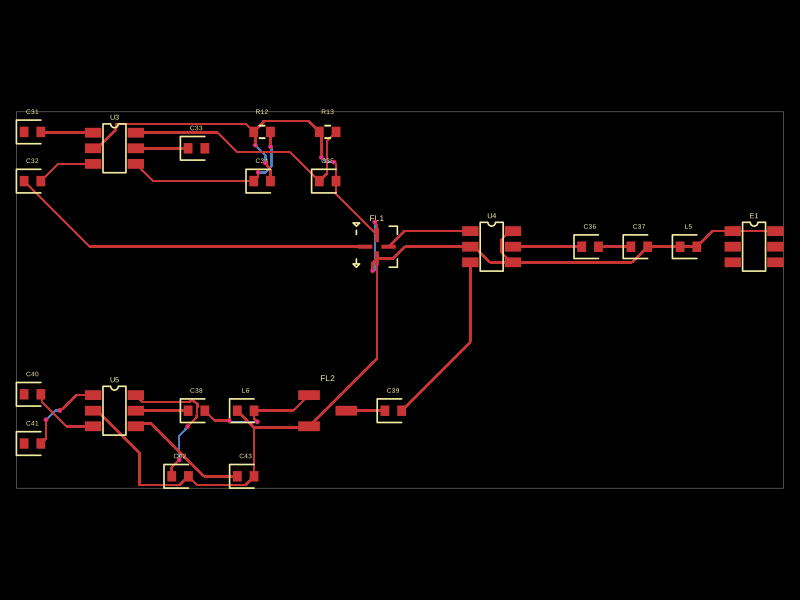 Similar packageMustafaMulla29/CC3235SF-tsxThis code defines a PCB layout with RF front-end components including RF switches (RTC6608OSP), band-pass filters, a diplexer, matching capacitors and inductors, and an antenna, all arranged to match a specific schematic for high-frequency radio signal routing.
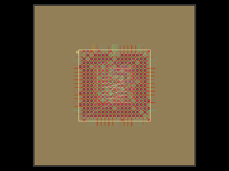 Discover something new0hmX/am3352This code defines a six-layer printed circuit board (PCB) design with a TI AM3352 microprocessor package, including precise pin mapping, power plane definition, fixed component placement, and PCB layout visualization.