imrishabh18/fitness_watch
This circuit integrates an ESP-12E microcontroller with various sensors and peripherals, including a AO3400A MOSFET for switching loads, to enable wireless control and sensor data processing.
- Version
- 1.0.12
- License
- unset
- Stars
- 1
index.circuit.tsx
PCB
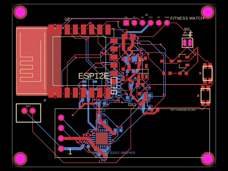
Schematic

import { replayReviewedRoutes } from "./reviewed-routing"
import { MAX30102EFD_T } from "./imports/MAX30102EFD_T/MAX30102EFD_T"
import { MPU_6050 } from "./imports/MPU_6050/MPU_6050"
import { LCM1027A2445F } from "./imports/LCM1027A2445F/LCM1027A2445F"
import { HS91L02W2C01 } from "./imports/HS91L02W2C01/HS91L02W2C01"
import { TLV70018DDCR } from "./imports/TLV70018DDCR/TLV70018DDCR"
import { A_0603B222K500NT } from "./imports/A_0603B222K500NT/A_0603B222K500NT"
import { A_0603B103K500NT } from "./imports/A_0603B103K500NT/A_0603B103K500NT"
import { CL10A475KO8NNNC } from "./imports/CL10A475KO8NNNC/CL10A475KO8NNNC"
import { A_0603WAF4701T5E } from "./imports/A_0603WAF4701T5E/A_0603WAF4701T5E"
import diodeObj from "./models/jlcpcb-C191023-1n5819ws.obj"
import switchObj from "./models/jlcpcb-C202420-switch.obj"
import header1x6Obj from "./models/jlcpcb-C541860-header-1x6.obj"
import resistor0603Obj from "./imports/A_0603WAF1002T5E/A_0603WAF1002T5E.obj"
import capacitor0603Obj from "./imports/CC0603KRX7R6BB105/CC0603KRX7R6BB105.obj"
import capacitor0805Obj from "./imports/FCC0805X106K100FT/FCC0805X106K100FT.obj"
import { AO3400A } from "./imports/AO3400A"
import { AP2112K_3_3TRG1 } from "./imports/AP2112K_3_3TRG1/AP2112K_3_3TRG1"
import { B2B_PH_K_S_LF__SN_ } from "./imports/B2B_PH_K_S_LF__SN_"
import { ESP_12E } from "./imports/ESP_12E/ESP_12E"


// Local copies of the exact JLCPCB package models keep the dev viewer and
// offline fabrication exports independent of the model CDN.
const jlc0603ResistorCadModel = {
  objUrl: resistor0603Obj,
  pcbRotationOffset: 90,
  modelOriginPosition: { x: -0.005, y: 0, z: -0.01 },
} as const

const jlc0603CapacitorCadModel = {
  objUrl: capacitor0603Obj,
  pcbRotationOffset: 0,
  modelOriginPosition: { x: 0, y: 0, z: -0.4 },
} as const

const jlc0805CapacitorCadModel = {
  objUrl: capacitor0805Obj,
  pcbRotationOffset: 0,
  modelOriginPosition: { x: 0, y: -0.0000127, z: -0.65 },
} as const


const Jlc0603ResistorFootprint = () => (
  <footprint originalLayer="top">
    <courtyardrect pcbX={0} pcbY={0} width="2.5mm" height="1.1mm" />
    <smtpad shape="rect" width="0.8064754mm" height="0.8640064mm" pcbX="-0.753364mm" pcbY={0} portHints={["pin1"]} />
    <smtpad shape="rect" width="0.8064754mm" height="0.8640064mm" pcbX="0.753364mm" pcbY={0} portHints={["pin2"]} />
  </footprint>
)

const Jlc0603CapacitorFootprint = () => (
  <footprint originalLayer="top">
    <courtyardrect pcbX={0} pcbY={0} width="2.5mm" height="1.2mm" />
    <smtpad shape="rect" width="0.7999984mm" height="0.8999982mm" pcbX="-0.700024mm" pcbY={0} portHints={["pin1"]} />
    <smtpad shape="rect" width="0.7999984mm" height="0.8999982mm" pcbX="0.700024mm" pcbY={0} portHints={["pin2"]} />
  </footprint>
)

const Jlc0805CapacitorFootprint = () => (
  <footprint originalLayer="top">
    <courtyardrect pcbX={0} pcbY={0} width="3.7mm" height="1.65mm" />
    <smtpad shape="rect" width="1.4100048mm" height="1.35001mm" pcbX="-0.999998mm" pcbY={0} portHints={["pin1"]} />
    <smtpad shape="rect" width="1.4100048mm" height="1.35001mm" pcbX="0.999998mm" pcbY={0} portHints={["pin2"]} />
  </footprint>
)

const JlcDiodeC191023Footprint = () => (
  <footprint originalLayer="top">
    <courtyardrect pcbX={0} pcbY={0} width="3.85mm" height="1.3mm" />
    <smtpad
      shape="rect"
      width="1mm"
      height="0.7mm"
      pcbX="-1.172464mm"
      pcbY={0}
      portHints={["pin1"]}
    />
    <smtpad
      shape="rect"
      width="1mm"
      height="0.7mm"
      pcbX="1.172464mm"
      pcbY={0}
      portHints={["pin2"]}
    />
  </footprint>
)

const JlcSwitchC202420Footprint = () => (
  <footprint originalLayer="top">
    <courtyardrect pcbX={0} pcbY={0} width="5.0002mm" height="3.1501mm" />
    <smtpad shape="rect" width="1.4mm" height="0.9mm" pcbX="-1.800098mm" pcbY="-1.125042mm" portHints={["pin1"]} />
    <smtpad shape="rect" width="1.4mm" height="0.9mm" pcbX="1.800098mm" pcbY="-1.125042mm" portHints={["pin2"]} />
    <smtpad shape="rect" width="1.4mm" height="0.9mm" pcbX="-1.800098mm" pcbY="0.17493mm" portHints={["pin3"]} />
    <smtpad shape="rect" width="1.4mm" height="0.9mm" pcbX="1.800098mm" pcbY="0.17493mm" portHints={["pin4"]} />
    <smtpad shape="rect" width="0.6mm" height="0.5mm" pcbX={0} pcbY="1.325042mm" portHints={["pin5"]} />
    <silkscreenrect
      pcbX={0}
      pcbY="-0.475mm"
      width="3.5mm"
      height="2.2mm"
      filled={false}
      stroke="solid"
      strokeWidth="0.2mm"
    />
  </footprint>
)

const JstPh2BatteryFootprint = () => (
  <footprint originalLayer="top">
    <courtyardrect pcbX={0} pcbY="-0.55mm" width="6.5mm" height="5mm" />
    {/* C131337 identifies pin 1 on the right when viewed from the top. */}
    <platedhole shape="circle" holeDiameter="0.9mm" outerDiameter="1.6mm" pcbX="1mm" pcbY={0} portHints={["pin1"]} />
    <platedhole shape="circle" holeDiameter="0.9mm" outerDiameter="1.6mm" pcbX="-1mm" pcbY={0} portHints={["pin2"]} />
    <silkscreenrect pcbX={0} pcbY="-0.55mm" width="6mm" height="4.5mm" filled={false} stroke="solid" strokeWidth="0.2mm" />
    <silkscreentext text="BAT" pcbX={0} pcbY="1.1mm" fontSize="0.6mm" />
  </footprint>
)

export default () => (
  <board
    title="ESP8266 Fitness Watch"
    width="50mm"
    height="40mm"
    thickness="1.6mm"
    borderRadius="2mm"
    layers={2}
    solderMaskColor="black"
    silkscreenColor="white"
    doubleSidedAssembly
    autorouter={{ local: true, algorithmFn: replayReviewedRoutes }}
    pcbStyle={{ viaPadDiameter: "0.5mm", viaHoleDiameter: "0.25mm" }}
  >
    <net name="GND" isGroundNet />
    <net name="VBAT" />
    <net name="V3V3" />
    <net name="I2C_SCL" />
    <net name="I2C_SDA" />
    <net name="MOTOR_LOW" />
    <net name="V1V8" />
    <net name="HR_INT" />
    <net name="MOTION_INT" />

    {/* Four non-plated M2-class band/case mounting holes on dedicated
        upper and lower side rails. A 1.7 mm keepout radius provides 0.5 mm
        copper clearance around each 2.4 mm drill on both layers. */}
    <hole name="H1" diameter="2.4mm" pcbX={-23} pcbY={18} />
    <hole name="H2" diameter="2.4mm" pcbX={23} pcbY={18} />
    <hole name="H3" diameter="2.4mm" pcbX={-23} pcbY={-18} />
    <hole name="H4" diameter="2.4mm" pcbX={23} pcbY={-18} />
    <keepout shape="circle" radius="1.7mm" pcbX={-23} pcbY={18} layers={["top", "bottom"]} />
    <keepout shape="circle" radius="1.7mm" pcbX={23} pcbY={18} layers={["top", "bottom"]} />
    <keepout shape="circle" radius="1.7mm" pcbX={-23} pcbY={-18} layers={["top", "bottom"]} />
    <keepout shape="circle" radius="1.7mm" pcbX={23} pcbY={-18} layers={["top", "bottom"]} />

    {/* Functional schematic regions. Cross-section nets are rendered as
        labeled connections, keeping each block compact and readable. */}
    <schematicsection name="regulation" displayName="Battery & 3.3 V Regulation" sectionTitleFontSize="0.34mm" />
    <schematicsection name="controller" displayName="ESP8266 Core, Controls & Motor" sectionTitleFontSize="0.34mm" />
    <schematicsection name="peripherals" displayName="Display, Motion & Pulse Sensors" sectionTitleFontSize="0.34mm" />


    {/* ESP8266 core. The antenna faces the left edge, with copper kept away. */}
    <ESP_12E
      name="U2"
      manufacturerPartNumber="ESP-12E"
      pcbX={-7.625}
      pcbY={6}
      pcbRotation={0}
      schSectionName="controller"
      schX={-7.5}
      schY={-2.5}
      schWidth="4mm"
      schHeight="6mm"
      schPinStyle={{
        ADC: { marginTop: "0.14mm" },
        EN: { marginTop: "0.14mm" },
        GPIO16: { marginTop: "0.14mm" },
        GPIO14: { marginTop: "0.14mm" },
        GPIO12: { marginTop: "0.14mm" },
        GPIO13: { marginTop: "0.14mm" },
        VCC: { marginTop: "0.14mm" },
        RXD: { marginTop: "0.14mm" },
        GPIO5: { marginTop: "0.14mm" },
        GPIO4: { marginTop: "0.14mm" },
        GPIO0: { marginTop: "0.14mm" },
        GPIO2: { marginTop: "0.14mm" },
        GPIO15: { marginTop: "0.14mm" },
        GND: { marginTop: "0.14mm" },
        MISO: { marginLeft: "0.14mm" },
        GPIO9: { marginLeft: "0.14mm" },
        GPIO10: { marginLeft: "0.14mm" },
        MOSI: { marginLeft: "0.14mm" },
        SCLK: { marginLeft: "0.14mm" },
      }}
      schPinArrangement={{
        leftSide: [
          "RESET",
          "ADC",
          "EN",
          "GPIO16",
          "GPIO14",
          "GPIO12",
          "GPIO13",
          "VCC",
        ],
        rightSide: [
          "TXD",
          "RXD",
          "GPIO5",
          "GPIO4",
          "GPIO0",
          "GPIO2",
          "GPIO15",
          "GND",
        ],
        bottomSide: ["CS0", "MISO", "GPIO9", "GPIO10", "MOSI", "SCLK"],
      }}
      noConnect={[
        "GPIO16",
        "ADC",
        "CS0",
        "MISO",
        "GPIO9",
        "GPIO10",
        "MOSI",
        "SCLK",
      ]}
    />
    <keepout
      shape="rect"
      pcbX={-18.5}
      pcbY={6}
      width="11mm"
      height="17mm"
      layers={["top", "bottom"]}
      excludeRefs={[".U2"]}
    />

    {/* Strict copper keepout under the printed antenna itself. The original
        larger clearance region also covers module pads and excludes U2. */}
    <keepout shape="rect" pcbX={-20.25} pcbY={6} width="7.5mm"
      height="17mm" layers={["top", "bottom"]} />

    {/* Battery input and 600 mA AP2112K 3.3 V regulator. */}
    <B2B_PH_K_S_LF__SN_
      name="J1"
      footprint={<JstPh2BatteryFootprint />}
      pcbX="-21mm"
      pcbY="-6.2mm"
      pcbRotation={0}
      schSectionName="regulation"
      schX={16}
      schY={11}
      schWidth="2.3mm"
      schHeight="1.7mm"
    />
    <AP2112K_3_3TRG1
      name="U1"
      pcbX="7mm"
      pcbY="3.5mm"
      schSectionName="regulation"
      schX={8}
      schY={11}
      schWidth="2.8mm"
      schHeight="2.1mm"
      schPinStyle={{ GND: { marginTop: "0.2mm" } }}
      schPinArrangement={{ leftSide: ["VIN", "GND", "EN"], rightSide: ["VOUT", "NC"] }}
      noConnect={["NC"]}
    />
    <capacitor name="C3" capacitance="1uF" manufacturerPartNumber="CC0603KRX7R6BB105" supplierPartNumbers={{ jlcpcb: ["C113807"] }} footprint={<Jlc0603CapacitorFootprint />} cadModel={jlc0603CapacitorCadModel} pcbX="6.4mm" pcbY="0.2mm" schSectionName="regulation" schX={5.5} schY={8} schRotation={90} />
    <capacitor name="C4" capacitance="1uF" manufacturerPartNumber="CC0603KRX7R6BB105" supplierPartNumbers={{ jlcpcb: ["C113807"] }} footprint={<Jlc0603CapacitorFootprint />} cadModel={jlc0603CapacitorCadModel} pcbX="7mm" pcbY="6.7mm" schSectionName="regulation" schX={10.5} schY={8} schRotation={90} />

    {/* Boot straps and user controls. */}
    <resistor name="R3" resistance="10k" manufacturerPartNumber="0603WAF1002T5E" supplierPartNumbers={{ jlcpcb: ["C25804"] }} footprint={<Jlc0603ResistorFootprint />} cadModel={jlc0603ResistorCadModel} pcbX="3mm" pcbY="6.5mm" schSectionName="controller" schX={-11.5} schY={-1} schRotation={90} />
    <resistor name="R4" resistance="10k" manufacturerPartNumber="0603WAF1002T5E" supplierPartNumbers={{ jlcpcb: ["C25804"] }} footprint={<Jlc0603ResistorFootprint />} cadModel={jlc0603ResistorCadModel} pcbX="3mm" pcbY="4mm" schSectionName="controller" schX={-3.7} schY={-4.5} schRotation={90} />
    <resistor name="R5" resistance="10k" manufacturerPartNumber="0603WAF1002T5E" supplierPartNumbers={{ jlcpcb: ["C25804"] }} footprint={<Jlc0603ResistorFootprint />} cadModel={jlc0603ResistorCadModel} pcbX="3mm" pcbY="1.5mm" schSectionName="controller" schX={-3.7} schY={-2.5} schRotation={90} />
    <resistor name="R6" resistance="10k" manufacturerPartNumber="0603WAF1002T5E" supplierPartNumbers={{ jlcpcb: ["C25804"] }} footprint={<Jlc0603ResistorFootprint />} cadModel={jlc0603ResistorCadModel} pcbX="7mm" pcbY="-2mm" schSectionName="controller" schX={-12.5} schY={-3} schRotation={90} />
    <pushbutton
      name="SW_RST"
      manufacturerPartNumber="SKSCPCE010"
      supplierPartNumbers={{ jlcpcb: ["C202420"] }}
      footprint={<JlcSwitchC202420Footprint />}
      cadModel={{
        objUrl: switchObj,
        // Center the C202420 body between the two custom footprint pads.
        modelOriginPosition: { x: 0, y: -0.17500000000000004, z: -0.01 },
      }}
      pinLabels={{ pin1: "RESET", pin2: "GND", pin3: "NC3", pin4: "NC4", pin5: "SHIELD" }}
      noConnect={["NC3", "NC4", "SHIELD"]}
      pcbX="22.5mm"
      pcbY="3mm"
      pcbRotation={90}
      schSectionName="controller"
      schX={-14}
      schY={-5}
    />
    <pushbutton
      name="SW_NAV"
      manufacturerPartNumber="SKSCPCE010"
      supplierPartNumbers={{ jlcpcb: ["C202420"] }}
      footprint={<JlcSwitchC202420Footprint />}
      cadModel={{
        objUrl: switchObj,
        // Center the C202420 body between the two custom footprint pads.
        modelOriginPosition: { x: 0, y: -0.17500000000000004, z: -0.01 },
      }}
      pinLabels={{ pin1: "GPIO0", pin2: "GND", pin3: "NC3", pin4: "NC4", pin5: "SHIELD" }}
      noConnect={["NC3", "NC4", "SHIELD"]}
      pcbX="22mm"
      pcbY="-2.5mm"
      pcbRotation={90}
      schSectionName="controller"
      schX={-4}
      schY={-7}
    />

    {/* JLCSearch parts. OLED is elevated above the top PCB; sensor faces skin. */}
    <HS91L02W2C01 name="DS1" pcbX={-13} pcbY={-11.7}
      schSectionName="peripherals" schX={13} schY={2} />
    <MPU_6050 name="U4" layer="bottom" pcbX={-3} pcbY={-13}
      schSectionName="peripherals" schX={13} schY={-5}
      noConnect={["NC1","NC2","NC3","NC4","NC5","NC6","NC7","NC8","AUX_DA","AUX_CL","RESV1","RESV2","RESV3"]} />
    {/* No copper or vias beneath the MEMS die pad (TDK section 11.4). */}
    <keepout shape="rect" width="3mm" height="3mm" pcbX={-3} pcbY={-13}
      layers={["top", "bottom"]} />
    <MAX30102EFD_T name="U5" layer="bottom" pcbX={0} pcbY={0}
      schSectionName="peripherals" schX={22} schY={-5}
      noConnect={["pin1","pin5","pin6","pin7","pin8","pin14"]} />
    <TLV70018DDCR name="U6" layer="bottom" pcbX={-6} pcbY={0}
      schSectionName="regulation" schX={22} schY={11} noConnect={["NC"]} />
    <LCM1027A2445F name="M1" layer="top" pcbRotation={0} pcbX={18} pcbY={10.5}
      schSectionName="controller" schX={-15.5} schY={-13.5} />
    {/* GPIO0 boot strap and 100 kHz shared I2C bus pull-ups. */}
    <resistor name="R14" resistance="10k" manufacturerPartNumber="0603WAF1002T5E"
      supplierPartNumbers={{jlcpcb:["C25804"]}} footprint={<Jlc0603ResistorFootprint />}
      cadModel={jlc0603ResistorCadModel} pcbX={10} pcbY={-6}
      schSectionName="controller" schX={-1} schY={-7} />
    <A_0603WAF4701T5E name="R15" pcbX={8} pcbY={-2.5} layer="bottom"
      schSectionName="peripherals" schX={17} schY={3} />
    <A_0603WAF4701T5E name="R16" pcbX={8} pcbY={-5.5} layer="bottom"
      schSectionName="peripherals" schX={20} schY={3} />
    <A_0603WAF4701T5E name="R17" pcbX={5} pcbY={0} layer="bottom"
      schSectionName="peripherals" schX={25} schY={3} />
    <A_0603B222K500NT name="C10" pcbX={-3} pcbY={-9} layer="bottom"
      schSectionName="peripherals" schX={11} schY={-12} />
    <A_0603B103K500NT name="C11" pcbX={-3} pcbY={-17} layer="bottom"
      schSectionName="peripherals" schX={14} schY={-12} />
    <CL10A475KO8NNNC name="C15" pcbX={-3} pcbY={-4.4} layer="bottom"
      schSectionName="peripherals" schX={24} schY={-12} />
    <capacitor name="C8" capacitance="100nF" manufacturerPartNumber="CC0603KRX7R9BB104"
      supplierPartNumbers={{jlcpcb:["C14663"]}} footprint={<Jlc0603CapacitorFootprint />}
      cadModel={jlc0603CapacitorCadModel} pcbX={-7} pcbY={-15} layer="bottom"
      schSectionName="peripherals" schX={8} schY={-15} />
    <capacitor name="C9" capacitance="100nF" manufacturerPartNumber="CC0603KRX7R9BB104"
      supplierPartNumbers={{jlcpcb:["C14663"]}} footprint={<Jlc0603CapacitorFootprint />}
      cadModel={jlc0603CapacitorCadModel} pcbX={1} pcbY={-11} layer="bottom"
      schSectionName="peripherals" schX={17} schY={-15} />
    <capacitor name="C13" capacitance="100nF" manufacturerPartNumber="CC0603KRX7R9BB104"
      supplierPartNumbers={{jlcpcb:["C14663"]}} footprint={<Jlc0603CapacitorFootprint />}
      cadModel={jlc0603CapacitorCadModel} pcbX={4} pcbY={3.5} layer="bottom"
      schSectionName="peripherals" schX={20} schY={-15} />
    <capacitor name="C16" capacitance="100nF" manufacturerPartNumber="CC0603KRX7R9BB104"
      supplierPartNumbers={{jlcpcb:["C14663"]}} footprint={<Jlc0603CapacitorFootprint />}
      cadModel={jlc0603CapacitorCadModel} pcbX={4} pcbY={-3} layer="bottom"
      schSectionName="peripherals" schX={27} schY={-15} />
    <capacitor name="C12" capacitance="10uF" manufacturerPartNumber="FCC0805X106K100FT"
      supplierPartNumbers={{jlcpcb:["C5137471"]}} footprint={<Jlc0805CapacitorFootprint />}
      cadModel={jlc0805CapacitorCadModel} pcbX={4} pcbY={6.5} layer="bottom"
      schSectionName="peripherals" schX={21} schY={-12} />
    <capacitor name="C14" capacitance="1uF" manufacturerPartNumber="CC0603KRX7R6BB105"
      supplierPartNumbers={{jlcpcb:["C113807"]}} footprint={<Jlc0603CapacitorFootprint />}
      cadModel={jlc0603CapacitorCadModel} pcbX={-7} pcbY={-3.5} layer="bottom"
      schSectionName="peripherals" schX={21} schY={-15} />
    <AO3400A
      name="Q1"
      pcbX="17mm"
      pcbY="6mm"
      schSectionName="controller"
      schX={-9.5}
      schY={-13.5}
      schWidth="2.6mm"
      schHeight="2.1mm"
      schPinArrangement={{ leftSide: ["G"], rightSide: ["D", "S"] }}
    />
    <resistor name="R9" resistance="100" manufacturerPartNumber="0603WAF1000T5E" supplierPartNumbers={{ jlcpcb: ["C22775"] }} footprint={<Jlc0603ResistorFootprint />} cadModel={jlc0603ResistorCadModel} pcbX="13mm" pcbY="3mm" schSectionName="controller" schX={-7.5} schY={-11} />
    <resistor name="R13" resistance="100k" manufacturerPartNumber="0603WAF1003T5E" supplierPartNumbers={{ jlcpcb: ["C25803"] }} footprint={<Jlc0603ResistorFootprint />} cadModel={jlc0603ResistorCadModel} pcbX="17mm" pcbY="3mm" schSectionName="controller" schX={-8} schY={-15.5} schRotation={90} />
    <diode
      name="D2"
      variant="schottky"
      manufacturerPartNumber="1N5819WS"
      supplierPartNumbers={{ jlcpcb: ["C191023"] }}
      footprint={<JlcDiodeC191023Footprint />}
      pinLabels={{ pin1: "CATHODE", pin2: "ANODE" }}
      cadModel={{
        objUrl: diodeObj,
        modelOriginPosition: { x: 0, y: 0.00011430000006384944, z: 0 },
      }}
      pcbX="13mm"
      pcbY="6mm"
      pcbRotation={180}
      schSectionName="controller"
      schX={-12.5}
      schY={-11}
    />

    {/* FTDI-compatible serial programming header from the reference schematic. */}
    <pinheader
      name="J2"
      pinAttributes={{pin1:{doNotConnect:true},pin5:{doNotConnect:true}}}
      manufacturerPartNumber="PZ200V-11-06P"
      supplierPartNumbers={{ jlcpcb: ["C541860"] }}
      cadModel={{
        objUrl: header1x6Obj,
        modelOriginPosition: { x: 0, y: 0, z: 0.19999400000000023 },
      }}
      pinCount={6}
      pitch="2mm"
      gender="male"
      pinLabels={["NC1", "ESP_TX", "ESP_RX", "VCC_3V3", "NC2", "GND"]}
      pcbPinLabels={{ pin1: "NC", pin2: "TX", pin3: "RX", pin4: "3V3", pin5: "NC", pin6: "GND" }}
      showSilkscreenPinLabels
      pcbX="8mm"
      pcbY="15.4mm"
      schSectionName="controller"
      schX={-4.5}
      schY={-13.5}
      schWidth="2.5mm"
      schHeight="3.4mm"
      schPinStyle={{
        ESP_TX: { marginTop: "0.15mm" },
        ESP_RX: { marginTop: "0.15mm" },
        VCC_3V3: { marginTop: "0.15mm" },
        NC2: { marginTop: "0.15mm" },
        GND: { marginTop: "0.15mm" },
      }}
    />

    {/* Local 3.3 V decoupling near the ESP-12E. */}
    <capacitor name="C6" capacitance="100nF" manufacturerPartNumber="CC0603KRX7R9BB104" supplierPartNumbers={{ jlcpcb: ["C14663"] }} footprint={<Jlc0603CapacitorFootprint />} cadModel={jlc0603CapacitorCadModel} pcbX="3mm" pcbY="9mm" schSectionName="controller" schX={-11.5} schY={2} schRotation={90} />
    <capacitor name="C7" capacitance="10uF" manufacturerPartNumber="FCC0805X106K100FT" supplierPartNumbers={{ jlcpcb: ["C5137471"] }} footprint={<Jlc0805CapacitorFootprint />} cadModel={jlc0805CapacitorCadModel} pcbX="3.6mm" pcbY="12mm" schSectionName="controller" schX={-4} schY={2} schRotation={90} />

    {/* Battery and regulated rail. */}
    <trace name="T035" from=".J1 > .pin1" to="net.VBAT" width="0.8mm" />
    <trace name="T036" from=".J1 > .pin2" to="net.GND" width="0.8mm" />
    <trace name="T037" from=".U1 > .VIN" to="net.VBAT" width="0.8mm" />
    <trace name="T038" from=".U1 > .EN" to="net.VBAT" width="0.3mm" />
    <trace name="T039" from=".U1 > .VOUT" to="net.V3V3" width="0.8mm" />
    <trace name="T040" from=".U1 > .GND" to="net.GND" width="0.5mm" />
    <trace name="T041" from=".C3 > .pin1" to="net.VBAT" width="0.4mm" />
    <trace name="T042" from=".C3 > .pin2" to="net.GND" width="0.4mm" />
    <trace name="T043" from=".C4 > .pin1" to="net.V3V3" width="0.4mm" />
    <trace name="T044" from=".C4 > .pin2" to="net.GND" width="0.4mm" />

    {/* ESP power, boot straps, buttons, and serial programming. */}
    <trace name="T045" from=".U2 > .pin8" to="net.V3V3" width="0.5mm" />
    <trace name="T046" from=".U2 > .pin15" to="net.GND" width="0.5mm" />
    <trace name="T047" from=".U2 > .pin3" to=".R3 > .pin1" />
    <trace name="T048" from=".R3 > .pin2" to="net.V3V3" />
    <trace name="T049" from=".U2 > .pin16" to=".R4 > .pin1" />
    <trace name="T050" from=".R4 > .pin2" to="net.GND" />
    <trace name="T051" from=".U2 > .pin17" to=".R5 > .pin1" />
    <trace name="T052" from=".R5 > .pin2" to="net.V3V3" />
    <trace name="T053" from=".U2 > .pin1" to=".R6 > .pin1" />
    <trace name="T054" from=".R6 > .pin2" to="net.V3V3" />
    <trace name="T055" from=".U2 > .pin1" to=".SW_RST > .pin1" />
    <trace name="T056" from=".SW_RST > .pin2" to="net.GND" />
    <trace name="T057" from=".U2 > .pin18" to=".SW_NAV > .pin1" />
    <trace name="T058" from=".SW_NAV > .pin2" to="net.GND" />
    <trace name="T059" from=".U2 > .pin22" to=".J2 > .pin2" />
    <trace name="T060" from=".U2 > .pin21" to=".J2 > .pin3" />
    <trace name="T061" from=".J2 > .pin4" to="net.V3V3" width="0.4mm" />
    <trace name="T062" from=".J2 > .pin6" to="net.GND" width="0.4mm" />
    <trace name="T063" from=".C6 > .pin1" to="net.V3V3" />
    <trace name="T064" from=".C6 > .pin2" to="net.GND" />
    <trace name="T065" from=".C7 > .pin1" to="net.V3V3" width="0.4mm" />
    <trace name="T066" from=".C7 > .pin2" to="net.GND" width="0.4mm" />

    {/* Shared I2C bus. */}
    <trace name="T067" from=".U2 > .pin20" to="net.I2C_SCL" />
    <trace name="T068" from=".U2 > .pin19" to="net.I2C_SDA" />
    <trace name="T069" from=".DS1 > .pin3" to="net.I2C_SCL" />
    <trace name="T070" from=".DS1 > .pin4" to="net.I2C_SDA" />
    <trace name="T071" from=".DS1 > .pin2" to="net.V3V3" width="0.4mm" />
    <trace name="T072" from=".DS1 > .pin1" to="net.GND" width="0.4mm" />
    {/* Bare sensor power, bypass capacitors, interrupts and address straps. */}
    <trace name="T073" from=".U4 > .pin23" to="net.I2C_SCL" />
    <trace name="T074" from=".U5 > .pin2" to="net.I2C_SCL" />
    <trace name="T075" from=".R15 > .pin1" to="net.I2C_SCL" />
    <trace name="T076" from=".U4 > .pin24" to="net.I2C_SDA" />
    <trace name="T077" from=".U5 > .pin3" to="net.I2C_SDA" />
    <trace name="T078" from=".R16 > .pin1" to="net.I2C_SDA" />
    <trace name="T079" from=".U4 > .pin8" to="net.V3V3" />
    <trace name="T080" from=".U4 > .pin13" to="net.V3V3" />
    <trace name="T081" from=".U5 > .pin9" to="net.V3V3" />
    <trace name="T082" from=".U5 > .pin10" to="net.V3V3" />
    <trace name="T083" from=".U6 > .pin1" to="net.V3V3" />
    <trace name="T084" from=".U6 > .pin3" to="net.V3V3" />
    <trace name="T085" from=".R14 > .pin2" to="net.V3V3" />
    <trace name="T086" from=".R15 > .pin2" to="net.V3V3" />
    <trace name="T087" from=".R16 > .pin2" to="net.V3V3" />
    <trace name="T088" from=".R17 > .pin2" to="net.V3V3" />
    <trace name="T089" from=".C9 > .pin1" to="net.V3V3" />
    <trace name="T090" from=".C11 > .pin1" to="net.V3V3" />
    <trace name="T091" from=".C12 > .pin1" to="net.V3V3" />
    <trace name="T092" from=".C13 > .pin1" to="net.V3V3" />
    <trace name="T093" from=".C14 > .pin1" to="net.V3V3" />
    <trace name="T094" from=".U6 > .pin5" to="net.V1V8" />
    <trace name="T095" from=".U5 > .pin11" to="net.V1V8" />
    <trace name="T096" from=".C15 > .pin1" to="net.V1V8" />
    <trace name="T097" from=".C16 > .pin1" to="net.V1V8" />
    <trace name="T098" from=".U4 > .pin1" to="net.GND" />
    <trace name="T099" from=".U4 > .pin9" to="net.GND" />
    <trace name="T100" from=".U4 > .pin11" to="net.GND" />
    <trace name="T101" from=".U4 > .pin18" to="net.GND" />
    <trace name="T102" from=".U5 > .pin4" to="net.GND" />
    <trace name="T103" from=".U5 > .pin12" to="net.GND" />
    <trace name="T104" from=".U6 > .pin2" to="net.GND" />
    <trace name="T105" from=".C8 > .pin2" to="net.GND" />
    <trace name="T106" from=".C9 > .pin2" to="net.GND" />
    <trace name="T107" from=".C10 > .pin2" to="net.GND" />
    <trace name="T108" from=".C11 > .pin2" to="net.GND" />
    <trace name="T109" from=".C12 > .pin2" to="net.GND" />
    <trace name="T110" from=".C13 > .pin2" to="net.GND" />
    <trace name="T111" from=".C14 > .pin2" to="net.GND" />
    <trace name="T112" from=".C15 > .pin2" to="net.GND" />
    <trace name="T113" from=".C16 > .pin2" to="net.GND" />
    <trace name="T114" from=".U5 > .pin13" to="net.HR_INT" />
    <trace name="T115" from=".R17 > .pin1" to="net.HR_INT" />
    <trace name="T116" from=".U2 > .pin6" to="net.HR_INT" />
    <trace name="T117" from=".U4 > .pin12" to="net.MOTION_INT" />
    <trace name="T118" from=".U2 > .pin7" to="net.MOTION_INT" />
    <trace name="T119" from=".U4 > .pin10" to=".C8 > .pin1" />
    <trace name="T120" from=".U4 > .pin20" to=".C10 > .pin1" />
    <trace name="T121" from=".U2 > .pin18" to=".R14 > .pin1" />

    {/* Haptic motor driver. */}
    <trace name="T122" from=".U2 > .pin5" to=".R9 > .pin1" />
    <trace name="T123" from=".R9 > .pin2" to=".Q1 > .G" />
    <trace name="T124" from=".R13 > .pin1" to=".Q1 > .G" />
    <trace name="T125" from=".R13 > .pin2" to="net.GND" />
    <trace name="T126" from=".Q1 > .S" to="net.GND" width="0.5mm" />
    <trace name="T127" from=".Q1 > .D" to="net.MOTOR_LOW" width="0.6mm" />
    <trace name="T128" from=".M1 > .pin2" to="net.V3V3" width="0.6mm" />
    <trace name="T129" from=".M1 > .pin1" to="net.MOTOR_LOW" width="0.6mm" />
    <trace name="T130" from=".D2 > .ANODE" to="net.MOTOR_LOW" width="0.4mm" />
    <trace name="T131" from=".D2 > .CATHODE" to="net.V3V3" width="0.4mm" />

    <silkscreentext text="FITNESS WATCH" pcbX="18mm" pcbY="16.5mm" fontSize="1mm" anchorAlignment="center" />
    <silkscreentext text="EXT CHARGED 1S LIPO" pcbX="17mm" pcbY="-6mm" fontSize="0.55mm" anchorAlignment="center" />
    <silkscreentext text="ESP8266 / OLED / MPU6050" layer="bottom" pcbX={0} pcbY="-17mm" fontSize="0.8mm" anchorAlignment="bottom_center" />

  </board>
)
Related Packages
 More from this authorimrishabh18/boost-converterThis code defines a PCB schematic and 3D model layout focusing on a power conversion circuit with components like USB-C connector, MT3608 step-up regulator, inductor, diode, input/output capacitors, and resistors arranged on a double-layer PCB.
 Similar packagehrithik18k/smart-switch-pcbThe AO3400A component models a SOT-23 N-channel MOSFET with labeled pins for Gate, Source, and Drain, including 3D CAD models and schematic symbols for electronic circuit design.
 Discover something newShiboSoftwareDev/mspm0g3507-usb-c-dev-boardThe circuit assembles a USB-C port with integrated ESD protection, power regulation, UART interface, and microcontroller (MSPM0G3507) with supporting components for USB data lines, CC termination, I2C, SPI, reset circuitry, and indicator LEDs.