astra/f1c100s
The code defines the physical pin layout, labels, and footprint for the F1C100S system-on-chip (SoC) component used in electronic devices.
- Version
- 0.9.2
- License
- unset
- Stars
- 0
src/UnroutedModule.tsx
import { BreakoutTestPoint } from "./BreakoutTestPoint";
import { ClockCrystal } from "./ClockCrystal";
import { F1C100S } from "../imports/F1C100S";
import { makeLayout } from "./layout";
import type { LayoutProfile } from "./profiles";

export function UnroutedModule({
	layoutProfile,
}: {
	layoutProfile: LayoutProfile;
}) {
	const layout = makeLayout(layoutProfile);
	return (
		<group name="MODULE" pcbX={0} pcbY={0}>
			<F1C100S
				name="U1"
				pcbRotation={layout.rotation}
				schX={0}
				schY={0}
				schWidth={14}
				schHeight={24}
			/>
			<ClockCrystal placement={layout.crystal} />
			{layout.terminals.map((t) => (
				<BreakoutTestPoint key={t.name} terminal={t} />
			))}
			{layout.passives.map((p, i) =>
				p.kind === "capacitor" ? (
					<capacitor
						key={p.name}
						name={p.name}
						capacitance={p.value}
						maxVoltageRating={p.name.startsWith("C_OSC") ? 50 : 6.3}
						manufacturerPartNumber={
							p.name.startsWith("C_OSC") ? "GRM1555C1H180JA01D" : undefined
						}
						footprint="0402"
						layer="top"
						pcbX={p.x}
						pcbY={p.y}
						pcbRotation={p.rotation}
						schX={-22 + (i % 5) * 3}
						schY={18 - Math.floor(i / 5) * 3}
					/>
				) : (
					<resistor
						key={p.name}
						name={p.name}
						resistance={p.value}
						pcbRotation={p.rotation}
						footprint="0402"
						layer="top"
						pcbX={p.x}
						pcbY={p.y}
						schX={-22 + (i % 5) * 3}
						schY={18 - Math.floor(i / 5) * 3}
					/>
				),
			)}
			{/* maxLength bounds the aggregate multi-terminal rail tree. It is not a
        decoupling-loop constraint; power impedance still needs board-level review. */}
			{Object.entries(layout.nets).map(([name, ports]) => (
				<trace
					key={name}
					name={`N_${name}`}
					path={ports}
					thickness={0.12}
					maxLength={1000}
				/>
			))}
		</group>
	);
}
Related Packages
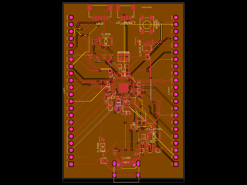 Similar packageabse/rp2350-mcu-boardThis code defines a compact, four-layer PCB hardware layout for the Raspberry Pi RP2350A microcontroller module, including the main IC, power regulation, USB-C connector, STM32-compatible headers, and associated passive components, with detailed component footprints, net connections, and copper pour zones for powering and ground references.
 Discover something newhrithik18k/smart-switch-pcbThe AO3400A component models a SOT-23 N-channel MOSFET with labeled pins for Gate, Source, and Drain, including 3D CAD models and schematic symbols for electronic circuit design.