astra/f1c100s
The code defines the physical pin layout, labels, and footprint for the F1C100S system-on-chip (SoC) component used in electronic devices.
- Version
- 0.9.2
- License
- unset
- Stars
- 0
scripts/validate.ts
import type { AnyCircuitElement } from "circuit-json";
import {
	runAllRoutingChecks,
	runAllPlacementChecks,
	checkViasInPads,
	checkEachPcbTraceNonOverlapping,
} from "@tscircuit/checks";
export async function validateCircuit(json: AnyCircuitElement[]) {
	const errors = [
		...(await runAllRoutingChecks(json)),
		...(await runAllPlacementChecks(json)),
		...checkViasInPads(json),
		...checkEachPcbTraceNonOverlapping(json, { minClearance: 0.1 }),
	].filter(
		(e: any) => e.type.endsWith("_error") || e.error_type?.endsWith("_error"),
	);
	const unique = [...new Map(errors.map((e: any) => [e.message, e])).values()];
	return unique;
}
export function circuitMetrics(json: AnyCircuitElement[]) {
	const traces = json.filter((e: any) => e.type === "pcb_trace") as any[];
	const length = (route: any[]) =>
		route.reduce((sum, p, i) => {
			const a = route[i - 1];
			return (
				sum +
				(a?.route_type === "wire" &&
				p.route_type === "wire" &&
				a.layer === p.layer
					? Math.hypot(a.x - p.x, a.y - p.y)
					: 0)
			);
		}, 0);
	const netTrace = (name: string) => {
		const source = json.find(
			(e: any) => e.type === "source_trace" && e.name === `N_${name}`,
		) as any;
		return traces.filter((t) => t.source_trace_id === source?.source_trace_id);
	};
	const usb = { dm: netTrace("USB_DM"), dp: netTrace("USB_DP") };
	const usbLength = (key: "dm" | "dp") =>
		usb[key].reduce((n, t) => n + length(t.route), 0);
	if (
		usb.dm.length !== 1 ||
		usb.dp.length !== 1 ||
		[...usb.dm, ...usb.dp].some((t) =>
			t.route.some((p: any) => p.route_type !== "wire" || p.layer !== "top"),
		)
	)
		throw new Error("USB pair must use two uninterrupted top-layer traces");
	if (Math.abs(usbLength("dm") - usbLength("dp")) > 0.001)
		throw new Error("USB pair exceeds 1um local skew budget");
	const plated = json.filter((e) => e.type === "pcb_plated_hole") as any[];
	const nonTopExits = plated.filter((h) =>
		traces.some((t) =>
			[t.route[0], t.route.at(-1)].some(
				(p) => p.layer !== "top" && Math.hypot(p.x - h.x, p.y - h.y) < 1e-5,
			),
		),
	);
	return {
		platedTestPoints: plated.length,
		nonTopExitContacts: nonTopExits.length,
		traces: traces.length,
		wireSegments: traces.reduce(
			(sum, t) =>
				sum +
				t.route.filter((p: any, i: number, route: any[]) => {
					const a = route[i - 1];
					return (
						a?.route_type === "wire" &&
						p.route_type === "wire" &&
						a.layer === p.layer &&
						Math.hypot(a.x - p.x, a.y - p.y) > 1e-6
					);
				}).length,
			0,
		),
		vias: json.filter((e) => e.type === "pcb_via").length,
		capacitors: json.filter(
			(e: any) =>
				e.type === "source_component" && e.ftype === "simple_capacitor",
		).length,
		localDecouplers: json.filter(
			(e: any) => e.type === "source_component" && /^C_D\d+$/.test(e.name),
		).length,
		routedLengthMm: +traces
			.reduce((sum, t) => sum + length(t.route), 0)
			.toFixed(3),
		usbDmLengthMm: +usbLength("dm").toFixed(6),
		usbDpLengthMm: +usbLength("dp").toFixed(6),
		usbSkewMm: +Math.abs(usbLength("dm") - usbLength("dp")).toFixed(6),
	};
}
Related Packages
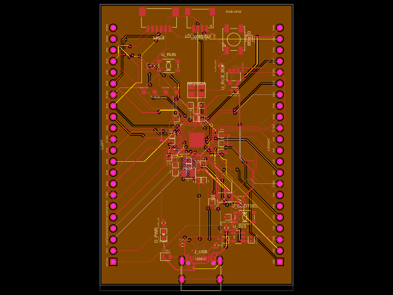 Similar packageabse/rp2350-mcu-boardThis code defines a compact, four-layer PCB hardware layout for the Raspberry Pi RP2350A microcontroller module, including the main IC, power regulation, USB-C connector, STM32-compatible headers, and associated passive components, with detailed component footprints, net connections, and copper pour zones for powering and ground references.
 Discover something newhrithik18k/smart-switch-pcbThe AO3400A component models a SOT-23 N-channel MOSFET with labeled pins for Gate, Source, and Drain, including 3D CAD models and schematic symbols for electronic circuit design.