astra/f1c100s
The code defines the physical pin layout, labels, and footprint for the F1C100S system-on-chip (SoC) component used in electronic devices.
- Version
- 0.9.2
- License
- unset
- Stars
- 0
docs/support-circuit-audit.md
# Processor support circuit audit

The module includes 32 capacitors, 13 resistors, and a 24 MHz crystal alongside the F1C100S. All fitted physical parts are on top. The 71 breakout exits are bare plated-hole test points, accessible on all four copper layers, with 0.45 mm copper diameter and 0.20 mm drill. This audit covers the local processor support network and the exposed SPI0, SDMMC0, and TWI0 buses; the carrier supplies regulated power, boot storage, and application-specific peripheral circuits.

## Reference circuits

The [Sipeed Lichee Nano schematic](https://dl.sipeed.com/LICHEE/Nano/HDK/lichee_nano_8.16%28Schematic%29.pdf) provides the reference for supply decoupling, reset, SDRAM reference, VRA references, TV references, and the 24 MHz oscillator. The TV network includes both reference-to-ground capacitors and the capacitor across the two reference pins. The module retains the original supply and reference networks and adds the missing cross-reference capacitor and oscillator.

The crystal is the [Abracon ABM8](https://abracon.com/Resonators/abm8.pdf), 24 MHz, 12 pF load variant. Its footprint follows the manufacturer's top-view land pattern: pins 1 and 3 are oscillator terminals; pins 2 and 4 connect to ground. Two 18 pF load capacitors assume 3 pF of effective stray capacitance: 18 × 18 / (18 + 18) + 3 = 12 pF. This is a design assumption to check by oscillator measurements on hardware. The loads use [Murata GRM1555C1H180JA01D](https://search.murata.co.jp/Ceramy/image/img/A01X/G101/ENG/GRM1555C1H180JA01-01.pdf), 18 pF ±5%, C0G, 50 V, 0402.

SD command/data pull-ups, the SPI chip-select pull-up, and I²C pull-ups establish idle states for the module's documented bus assignments. The I²C pull-ups are nominal 4.7 kΩ; their suitability depends on bus capacitance and operating speed, as described by the [NXP I²C specification](https://www.nxp.com/docs/en/user-guide/UM10204.pdf). No pull-up is fitted to the SD clock.

## Verification scope

Each of the five stored profiles is checked for trace clearance and connectivity, conventional horizontal/vertical/45° segments, top-layer component placement, oscillator connectivity and top-only routing, and the values and connections of the added support parts. The nonpolar ceramic decouplers place pin 1 (the supply/reference side) closer to the associated processor pin than pin 2. Dedicated C_D capacitors target their named supply pin; bulk and reference capacitors target the nearest processor pin on their supply/reference net. Crystal load capacitors retain their crystal-facing placement. This orientation is checked using emitted PCB port coordinates and electrical connectivity, including rotated module instances. The same checks run against the rendered module and built previews. Two rotated module instances and parent routing on each of the four layers are also exercised. Hole count, dimensions, exposed copper, layer connectivity, and the absence of duplicate drills or leftover surface pads are checked explicitly. These checks do not constitute power-integrity, signal-integrity, oscillator-startup, or hardware functional validation.
Related Packages
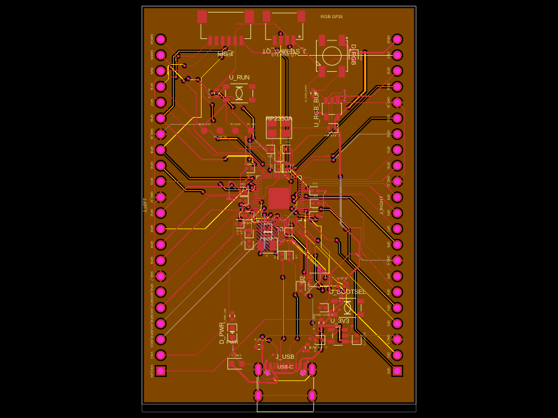 Similar packageabse/rp2350-mcu-boardThis code defines a compact, four-layer PCB hardware layout for the Raspberry Pi RP2350A microcontroller module, including the main IC, power regulation, USB-C connector, STM32-compatible headers, and associated passive components, with detailed component footprints, net connections, and copper pour zones for powering and ground references.
 Discover something newhrithik18k/smart-switch-pcbThe AO3400A component models a SOT-23 N-channel MOSFET with labeled pins for Gate, Source, and Drain, including 3D CAD models and schematic symbols for electronic circuit design.