abse/gameboy-advance
This code defines a collection of hardware components, including microcontrollers, sensors, display modules, power management ICs, and passive/passive components, each modeled as 3D symbols with specific footprints, pin configurations, and associated models for PCB and schematic design.
- Version
- 0.0.10
- License
- unset
- Stars
- 0
Microcontroller_RP2350_CrystalTop.circuit.tsx
PCB

Schematic

import { RP2350A } from "./imports/RP2350A"
import { W25Q16JVUXIQ } from "./imports/W25Q16JVUXIQ"
import { X322512MSB4SI } from "./imports/X322512MSB4SI"
import { SKRPACE010 } from "./imports/SKRPACE010"
import { AOTA_B201610S3R3_101_T } from "./imports/AOTA_B201610S3R3_101_T"
import { TYPE_C_16PIN_2MD_073_ } from "./imports/TYPE_C_16PIN_2MD_073_"
import { CL05B104KO5NNNC } from "./imports/CL05B104KO5NNNC"
import { CL05A475MP5NRNC } from "./imports/CL05A475MP5NRNC"
import { A_0402WGF1002TCE } from "./imports/A_0402WGF1002TCE"
import { A_0402WGF270JTCE } from "./imports/A_0402WGF270JTCE"
import { A_0402WGF5101TCE } from "./imports/A_0402WGF5101TCE"
import { A_0402WGF330JTCE } from "./imports/A_0402WGF330JTCE"
import { A_0402CG180J500NT } from "./imports/A_0402CG180J500NT"
import { Fragment } from "react"

type MicrocontrollerRP2350Props = {
  name?: string
  subcircuit?: boolean
  pcbX?: string | number
  pcbY?: string | number
  pcbRotation?: string | number
  schX?: string | number
  schY?: string | number
  schRotation?: string | number
}

const gndLabel = { displayName: "GND", schDisplayLabel: "GND" } as const
const v3v3Label = { displayName: "V3V3", schDisplayLabel: "V3V3" } as const
const v1v1Label = { displayName: "V1V1", schDisplayLabel: "V1V1" } as const
const vbusLabel = { displayName: "VBUS", schDisplayLabel: "VBUS" } as const
const denseTraceProps = { thickness: "0.1mm" } as const

const gpioNets = [
  "GPIO0", "GPIO1", "GPIO2", "GPIO3", "GPIO4", "GPIO5", "GPIO6",
  "GPIO7", "GPIO8", "GPIO9", "GPIO10", "GPIO11", "GPIO12", "GPIO13",
  "GPIO14", "GPIO15", "GPIO16", "GPIO17", "GPIO18", "GPIO19", "GPIO20",
  "GPIO21", "GPIO22", "GPIO23", "GPIO24", "GPIO25", "GPIO26_ADC0",
  "GPIO27_ADC1", "GPIO28_ADC2", "GPIO29_ADC3",
] as const

const parentRoutedGpios = new Set([
  // GPIO0/1 are I2C0 for the ER-TFT035IPS-6 capacitive-touch controller.
  // GPIO23 is its interrupt and GPIO24 controls the display backlight PWM.
  "GPIO0", "GPIO1", "GPIO2", "GPIO3", "GPIO4", "GPIO5", "GPIO6",
  "GPIO7", "GPIO8", "GPIO9", "GPIO10", "GPIO11", "GPIO16", "GPIO17",
  "GPIO18", "GPIO19", "GPIO20", "GPIO21", "GPIO22", "GPIO23", "GPIO24",
  // Storage bus: one shared SPI clock, dedicated microSD data/CS, and a
  // separate four-bit PSRAM data bus. All are routed by the parent board.
  "GPIO12", "GPIO13", "GPIO14", "GPIO15", "GPIO25", "GPIO26_ADC0",
  "GPIO27_ADC1", "GPIO28_ADC2", "GPIO29_ADC3",
])

const iovddPins = ["IOVDD1", "IOVDD2", "IOVDD3", "IOVDD4", "IOVDD5", "IOVDD6"] as const
const dvddPins = ["DVDD1", "DVDD2", "DVDD3"] as const

/**
 * Isolated crystal-placement experiment. It is a complete copy of the RP2350
 * MCU circuit so the working MCU implementation remains unchanged.
 */
export const Microcontroller_RP2350_CrystalTop = (props: MicrocontrollerRP2350Props) => (
  <group
    name="MICROCONTROLLER_RP2350_CRYSTAL_TOP"
    subcircuit={props.subcircuit ?? true}
    autorouter="auto"
    {...props}
  >
    <net name="GND" />
    <net name="VBUS" />
    <net name="V3V3" />
    <net name="V1V1" />

    <RP2350A
      name="U1"
      noConnect={gpioNets.filter((gpio) => !parentRoutedGpios.has(gpio))}
      showPinAliases
      schSectionName="rp2350"
      pcbX={0}
      pcbY={0}
      schX={0}
      schY={0}
      schWidth={2.8}
      schHeight={6.2}
    />

    <W25Q16JVUXIQ name="U2" schSectionName="flash" pcbX={-1.5} pcbY={7.9} schX={8} schY={0} schHeight={1} />
    {/* XIN/XOUT are on U1's lower edge. Keep the resonator and load caps on
        that same edge so the autorouter can use short, direct traces. */}
    <X322512MSB4SI name="U_XTAL" schSectionName="clock" pcbX={0} pcbY={-7} schX={-7.6} schY={6.2} />
    <SKRPACE010 name="U_BOOTSEL" schSectionName="controls" pcbX={10} pcbY={8.5} schX={8.5} schY={5.2} />
    <SKRPACE010 name="U_RUN" schSectionName="controls" pcbX={-10} pcbY={-2.5} schX={-9.05} schY={-4.6} />

    <TYPE_C_16PIN_2MD_073_
      name="J_USB"
      pinAttributes={{ B8: { doNotConnect: true }, A8: { doNotConnect: true } }}
      schSectionName="usb"
      pcbX={0}
      pcbY={-20}
      schX={11}
      schY={-5.5}
    />

    <AOTA_B201610S3R3_101_T name="U_CORE_INDUCTOR" schSectionName="power" pcbX={7.5} pcbY={-5.2} schX={9.5} schY={-4.5} />
    <A_0402WGF330JTCE name="R_VREG_AVDD" schSectionName="power" pcbX={5.5} pcbY={8.9} schX={-6.95} schY={-3.4} />
    <A_0402WGF1002TCE name="R_RUN" schSectionName="controls" pcbX={-9.5} pcbY={-8.1} schX={-5.65} schY={-4.6} />
    <A_0402WGF1002TCE name="R_BOOT" schSectionName="flash" pcbX={5.7} pcbY={6.6} schX={7.33} schY={4.2} />
    <A_0402WGF5101TCE name="R_CC1" schSectionName="usb" pcbX={-5.5} pcbY={-15} schX={7.2} schY={-5.2} />
    <A_0402WGF5101TCE name="R_CC2" schSectionName="usb" pcbX={5.5} pcbY={-15} schX={7.2} schY={-6.2} />
    <A_0402WGF270JTCE name="R_USB_DM" schSectionName="usb" pcbX={-1.2} pcbY={-12.4} schX={7.2} schY={-7.2} />
    <A_0402WGF270JTCE name="R_USB_DP" schSectionName="usb" pcbX={1.2} pcbY={-12.4} schX={7.2} schY={-8.2} />

    <CL05A475MP5NRNC name="C_VREG_IN" schSectionName="power" schOrientation="vertical" pcbX={-6.5} pcbY={-5.2} schX={-4.8} schY={-3.4} />
    <CL05A475MP5NRNC name="C_CORE" schSectionName="power" schOrientation="vertical" pcbX={9.5} pcbY={-7.2} schX={3.5} schY={-4.5} />
    <CL05A475MP5NRNC name="C_VREG_AVDD" maxDecouplingTraceLength={5.5} schSectionName="power" schOrientation="vertical" pcbX={2.3} pcbY={6} pcbRotation={90} schX={-6.45} schY={-2.4} />
    <CL05B104KO5NNNC name="C_IO" schSectionName="power" schOrientation="vertical" pcbX={-7} pcbY={3.8} schX={-6.4} schY={2.8} />
    <CL05B104KO5NNNC name="C_QSPI_USB" schSectionName="power" schOrientation="vertical" pcbX={5.6} pcbY={3.7} schX={6.01} schY={2.8} />
    <CL05B104KO5NNNC name="C_ADC" schSectionName="power" schOrientation="vertical" pcbX={10.5} pcbY={5.6} schX={5.36} schY={3.8} />
    <CL05B104KO5NNNC name="C_FLASH" schSectionName="flash" schOrientation="vertical" pcbX={8.5} pcbY={0} schX={9.4} schY={1.1} />
    <A_0402CG180J500NT name="C_XIN" schSectionName="clock" schOrientation="vertical" pcbX={-4} pcbY={-6.5} schX={-7.3} schY={7.4} />
    <A_0402CG180J500NT name="C_XOUT" schSectionName="clock" schOrientation="vertical" pcbX={4} pcbY={-6.5} schX={-5.7} schY={7.4} />
    <capacitor name="C_VBUS" capacitance="10uF" footprint="0603" schSectionName="usb" schOrientation="vertical" pcbX={0} pcbY={-16} schX={15} schY={-5.2} />

    <testpoint name="TP_SWDIO" footprintVariant="pad" padShape="circle" padDiameter="1.1mm" schSectionName="debug" pcbX={6} pcbY={-10} schX={-8.4} schY={-7.2} />
    <testpoint name="TP_SWCLK" footprintVariant="pad" padShape="circle" padDiameter="1.1mm" schSectionName="debug" pcbX={-6} pcbY={-10} schX={-6.4} schY={-7.2} />
    <testpoint name="TP_GND" footprintVariant="pad" padShape="circle" padDiameter="1.1mm" schSectionName="debug" pcbX={3} pcbY={-10} schX={-4.4} schY={-7.2} />
    <testpoint name="TP_3V3" footprintVariant="pad" padShape="circle" padDiameter="1.1mm" schSectionName="debug" pcbX={10} pcbY={-10} schX={-2.4} schY={-7.2} />

    <trace name="VREG_VIN" from=".U1 > .VREG_VIN" to="net.V3V3" {...v3v3Label} />
    <trace name="VREG_PGND" from=".U1 > .VREG_PGND" to="net.GND" {...gndLabel} />
    <trace name="VREG_LX" from=".U1 > .VREG_LX" to=".U_CORE_INDUCTOR > .pin1" />
    <trace name="CORE_OUT" from=".U_CORE_INDUCTOR > .pin2" to="net.V1V1" {...v1v1Label} />
    <trace name="VREG_FB" from=".U1 > .VREG_FB" to="net.V1V1" {...v1v1Label} />
    {dvddPins.map((pin) => <Fragment key={pin}><trace name={`${pin}_V1V1`} from={`.U1 > .${pin}`} to="net.V1V1" {...v1v1Label} /></Fragment>)}
    <trace name="C_VREG_IN_P" from=".C_VREG_IN > .pin1" to="net.V3V3" {...v3v3Label} />
    <trace name="C_VREG_IN_G" from=".C_VREG_IN > .pin2" to="net.GND" {...gndLabel} />
    <trace name="C_CORE_P" from=".C_CORE > .pin1" to="net.V1V1" {...v1v1Label} />
    <trace name="C_CORE_G" from=".C_CORE > .pin2" to="net.GND" {...gndLabel} />
    <trace name="VREG_AVDD_FILTER" from="net.V3V3" to=".R_VREG_AVDD > .pin1" {...v3v3Label} />
    <trace name="VREG_AVDD" from=".R_VREG_AVDD > .pin2" to=".U1 > .VREG_AVDD" />
    <trace name="C_VREG_AVDD_P" from=".C_VREG_AVDD > .pin1" to=".U1 > .VREG_AVDD" />
    <trace name="C_VREG_AVDD_G" from=".C_VREG_AVDD > .pin2" to="net.GND" maxLength="8mm" {...gndLabel} />

    {iovddPins.map((pin) => <Fragment key={pin}><trace name={`${pin}_V3V3`} from={`.U1 > .${pin}`} to="net.V3V3" {...v3v3Label} /></Fragment>)}
    <trace name="QSPI_IOVDD" from=".U1 > .QSPI_IOVDD" to="net.V3V3" {...v3v3Label} />
    <trace name="USB_OTP_VDD" from=".U1 > .USB_OTP_VDD" to="net.V3V3" {...v3v3Label} />
    <trace name="ADC_AVDD" from=".U1 > .ADC_AVDD" to="net.V3V3" {...v3v3Label} />
    <trace name="C_IO_P" from=".C_IO > .pin1" to="net.V3V3" {...v3v3Label} />
    <trace name="C_IO_G" from=".C_IO > .pin2" to="net.GND" {...gndLabel} />
    <trace name="C_QSPI_USB_P" from=".C_QSPI_USB > .pin1" to="net.V3V3" {...v3v3Label} />
    <trace name="C_QSPI_USB_G" from=".C_QSPI_USB > .pin2" to="net.GND" {...gndLabel} />
    <trace name="C_ADC_P" from=".C_ADC > .pin1" to="net.V3V3" {...v3v3Label} />
    <trace name="C_ADC_G" from=".C_ADC > .pin2" to="net.GND" {...gndLabel} />
    <trace name="GND_PAD" from=".U1 > .GND" to="net.GND" {...gndLabel} />

    <trace name="QSPI_SS" from=".U1 > .QSPI_SS" to=".U2 > .CS" {...denseTraceProps} />
    <trace name="QSPI_SD0" from=".U1 > .QSPI_SD0" to=".U2 > .pin5" {...denseTraceProps} />
    <trace name="QSPI_SD1" from=".U1 > .QSPI_SD1" to=".U2 > .pin2" {...denseTraceProps} />
    <trace name="QSPI_SD2" from=".U1 > .QSPI_SD2" to=".U2 > .pin3" {...denseTraceProps} />
    <trace name="QSPI_SD3" from=".U1 > .QSPI_SD3" to=".U2 > .pin7" {...denseTraceProps} />
    <trace name="QSPI_SCLK" from=".U1 > .QSPI_SCLK" to=".U2 > .CLK" {...denseTraceProps} />
    <trace name="FLASH_VCC" from=".U2 > .VCC" to="net.V3V3" {...v3v3Label} />
    <trace name="FLASH_GND" from=".U2 > .GND" to="net.GND" {...gndLabel} />
    <trace name="FLASH_EP" from=".U2 > .EP" to="net.GND" {...gndLabel} />
    <trace name="C_FLASH_P" from=".C_FLASH > .pin1" to="net.V3V3" {...v3v3Label} />
    <trace name="C_FLASH_G" from=".C_FLASH > .pin2" to="net.GND" {...gndLabel} />
    <trace name="BOOT_PULLUP" from=".R_BOOT > .pin1" to=".U1 > .QSPI_SS" />
    <trace name="BOOT_PULLUP_3V3" from=".R_BOOT > .pin2" to="net.V3V3" {...v3v3Label} />
    <trace name="BOOTSEL" from=".U_BOOTSEL > .pin1" to=".U1 > .QSPI_SS" />
    <trace name="BOOTSEL_GND" from=".U_BOOTSEL > .pin3" to="net.GND" {...gndLabel} />

    <trace name="XIN" from=".U_XTAL > .OSC1" to=".U1 > .XIN" />
    <trace name="XOUT" from=".U_XTAL > .OSC2" to=".U1 > .XOUT" />
    <trace name="XTAL_GND1" from=".U_XTAL > .GND1" to="net.GND" {...gndLabel} />
    <trace name="XTAL_GND2" from=".U_XTAL > .GND2" to="net.GND" {...gndLabel} />
    <trace name="T_C_XIN" from=".C_XIN > .pin1" to=".U1 > .XIN" />
    <trace name="C_XIN_GND" from=".C_XIN > .pin2" to="net.GND" {...gndLabel} />
    <trace name="T_C_XOUT" from=".C_XOUT > .pin1" to=".U1 > .XOUT" />
    <trace name="C_XOUT_GND" from=".C_XOUT > .pin2" to="net.GND" {...gndLabel} />
    <trace name="RUN_PULLUP" from=".R_RUN > .pin1" to=".U1 > .RUN" />
    <trace name="RUN_PULLUP_3V3" from=".R_RUN > .pin2" to="net.V3V3" {...v3v3Label} />
    <trace name="RUN_SWITCH" from=".U_RUN > .pin1" to=".U1 > .RUN" />
    <trace name="RUN_SWITCH_GND" from=".U_RUN > .pin3" to="net.GND" {...gndLabel} />
    <trace name="VBUS_A" from=".J_USB > .A4B9" to="net.VBUS" {...vbusLabel} />
    <trace name="VBUS_B" from=".J_USB > .B4A9" to="net.VBUS" {...vbusLabel} />
    <trace name="C_VBUS_P" from=".C_VBUS > .pin1" to="net.VBUS" {...vbusLabel} />
    <trace name="C_VBUS_G" from=".C_VBUS > .pin2" to="net.GND" {...gndLabel} />
    <trace name="USB_DM_A" from=".J_USB > .A7" to=".R_USB_DM > .pin1" />
    <trace name="USB_DM_B" from=".J_USB > .B7" to=".R_USB_DM > .pin1" />
    <trace name="USB_DM" from=".R_USB_DM > .pin2" to=".U1 > .USB_DM" {...denseTraceProps} />
    <trace name="USB_DP_A" from=".J_USB > .A6" to=".R_USB_DP > .pin1" />
    <trace name="USB_DP_B" from=".J_USB > .B6" to=".R_USB_DP > .pin1" />
    <trace name="USB_DP" from=".R_USB_DP > .pin2" to=".U1 > .USB_DP" {...denseTraceProps} />
    <trace name="CC1" from=".J_USB > .A5" to=".R_CC1 > .pin1" />
    <trace name="CC2" from=".J_USB > .B5" to=".R_CC2 > .pin1" />
    <trace name="CC1_GND" from=".R_CC1 > .pin2" to="net.GND" {...gndLabel} />
    <trace name="CC2_GND" from=".R_CC2 > .pin2" to="net.GND" {...gndLabel} />
    <trace name="USB_GND_A" from=".J_USB > .A1B12" to="net.GND" {...gndLabel} />
    <trace name="USB_GND_B" from=".J_USB > .B1A12" to="net.GND" {...gndLabel} />
    <trace name="USB_SHIELD_1" from=".J_USB > .EH1" to="net.GND" {...gndLabel} />
    <trace name="USB_SHIELD_1_ALT" from=".J_USB > .pin13_alt1" to="net.GND" {...gndLabel} />
    <trace name="USB_SHIELD_2" from=".J_USB > .EH2" to="net.GND" {...gndLabel} />
    <trace name="USB_SHIELD_2_ALT" from=".J_USB > .pin14_alt1" to="net.GND" {...gndLabel} />
    <trace name="SWDIO" from=".U1 > .SWDIO" to=".TP_SWDIO > .pin1" />
    <trace name="SWCLK" from=".U1 > .SWCLK" to=".TP_SWCLK > .pin1" />
    <trace name="T_TP_GND" from=".TP_GND > .pin1" to="net.GND" {...gndLabel} />
    <trace name="T_TP_3V3" from=".TP_3V3 > .pin1" to="net.V3V3" {...v3v3Label} />
  </group>
)
Related Packages
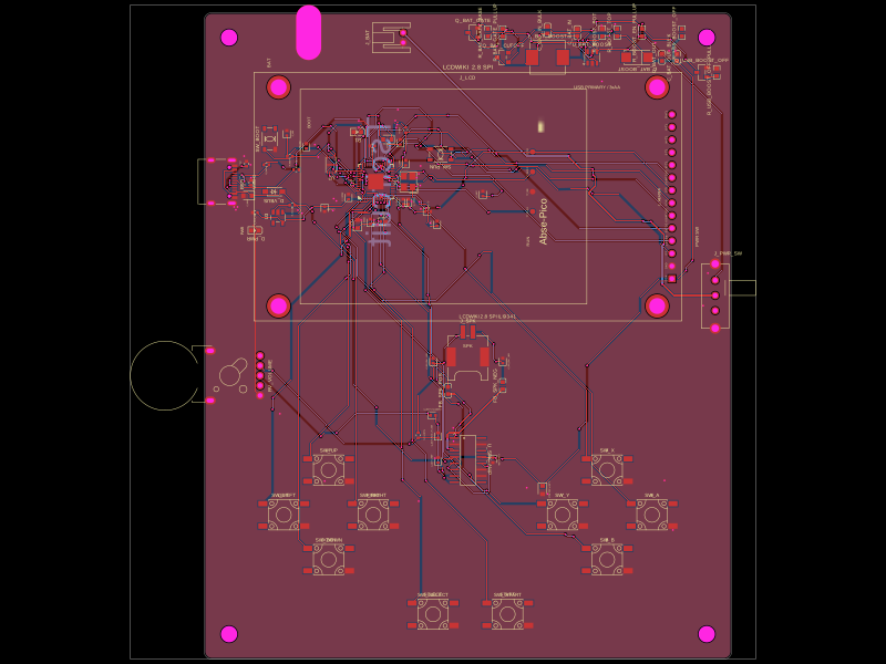 More from this authorabse/gameboyThis code defines the hardware mapping and schematic connections for a Raspberry Pi Pico-based development board featuring RP2040 microcontroller, USB-C connector, various power regulation components, decoupling capacitors, resistors, LEDs, headers, and supporting passive components for signal integrity and debugging.
 Similar packageaura/diy-power-delivery-triggerThis hardware design implements a USB Type-C port with supporting power management and signal conditioning components, including a USB-C connector, a FUSB302 USB-C port controller, ESD protection diodes, a buck converter for 3.3V power regulation, an STM32 microcontroller for control and processing, an RGB LED indicator, push button, terminal block connections, and associated filtering and support components.
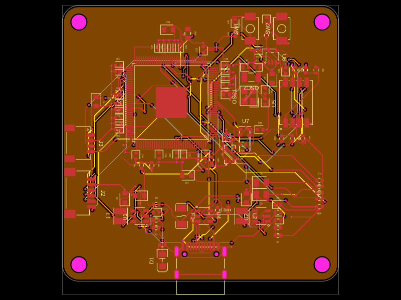 Discover something newtechmannih/trellis-coreThis code defines a detailed electronic hardware schematic and PCB layout for a Linux System-on-Module, incorporating components such as oscillators, power regulators, USB-C connectors, connectors, LEDs, resistors, capacitors, inductors, and integrated circuits, with precise physical footprint and 3D models.