ShiboSoftwareDev/am625sip-linux-board
This code defines the physical footprint and pin layout for an AM625 System-in-Package (SIP) component, detailing pad positions, pin labels, and package outline for hardware integration.
- Version
- 1.0.24
- License
- unset
- Stars
- 0
subcircuits/pmic-vsys.tsx
import { Fragment } from "react"
import { TPS6521908RHBR } from "../imports/TPS6521908RHBR"
import { WIP201610P_R47ML } from "../imports/WIP201610P_R47ML"

const PMIC_VSYS_REGION = {
  shape: "rect" as const,
  minX: 1.5,
  maxX: 19,
  minY: 12.5,
  maxY: 28,
}

/**
 * The 10 edges are the MST topology produced by the default autorouter for the
 * original 11-point VSYS_3V3 net. Routing one edge per phase avoids rebuilding
 * the expensive multi-point capacity mesh while preserving the same topology.
 */
export const PMIC_VSYS_LINKS = [
  [".U2 > .PVIN_B1_1", ".U2 > .PVIN_B1_2"],
  [".U2 > .PVIN_LDO1", ".U2 > .PVIN_B1_2"],
  [".R1 > .pin2", ".C5 > .pin1"],
  [".R2 > .pin2", ".C6 > .pin1"],
  [".C6 > .pin1", ".U2 > .VSYS"],
  [".U2 > .PVIN_LDO1", ".U2 > .VSYS"],
  [".R14 > .pin2", ".R2 > .pin2"],
  [".C5 > .pin1", ".U2 > .PVIN_B1_1"],
  [".C5 > .pin1", ".R13 > .pin2"],
  [".C3 > .pin1", ".U2 > .PVIN_LDO1"],
] as const

export const PmicVsysSubcircuit = () => (
  <subcircuit
    name="PMIC"
    pcbX={0}
    pcbY={0}
    width="28mm"
    height="18mm"
    autorouter="default"
  >
    {PMIC_VSYS_LINKS.map((_, index) => (
      <Fragment key={`PMIC_VSYS_ROUTE_PHASE_${index + 1}`}>
        <autoroutingphase
          name={`PMIC_VSYS_ROUTE_PHASE_${index + 1}`}
          phaseIndex={index}
          autorouter="default"
          region={PMIC_VSYS_REGION}
        />
      </Fragment>
    ))}

    <TPS6521908RHBR
      name="U2"
      pcbX={9}
      pcbY={20}
      pcbRotation={180}
    />
    <WIP201610P_R47ML
      name="L1"
      pcbX={14.5}
      pcbY={19.5}
      pcbRotation={270}
    />
    <WIP201610P_R47ML name="L2" pcbX={10} pcbY={14} />
    <WIP201610P_R47ML name="L3" pcbX={3.1} pcbY={15.8} />

    <capacitor
      name="C3"
      capacitance="4.7uF"
      maxVoltageRating="10V"
      footprint="0402"
      supplierPartNumbers={{ jlcpcb: ["C23733"] }}
      pcbX={18.5}
      pcbY={27}
    />
    <capacitor
      name="C4"
      capacitance="4.7uF"
      maxVoltageRating="10V"
      footprint="0402"
      supplierPartNumbers={{ jlcpcb: ["C23733"] }}
      pcbX={12.5}
      pcbY={16}
      pcbRotation={270}
    />
    <capacitor
      name="C5"
      capacitance="4.7uF"
      maxVoltageRating="10V"
      footprint="0402"
      supplierPartNumbers={{ jlcpcb: ["C23733"] }}
      pcbX={7}
      pcbY={15.3}
      pcbRotation={270}
    />
    <capacitor
      name="C6"
      capacitance="2.2uF"
      maxVoltageRating="6.3V"
      footprint="0201"
      supplierPartNumbers={{ jlcpcb: ["C6119760"] }}
      pcbX={7.5}
      pcbY={25}
    />
    <capacitor
      name="C7"
      capacitance="2.2uF"
      maxVoltageRating="6.3V"
      footprint="0201"
      supplierPartNumbers={{ jlcpcb: ["C6119760"] }}
      pcbX={8}
      pcbY={23.35}
      pcbRotation={180}
    />
    <capacitor
      name="C8"
      capacitance="2.2uF"
      maxVoltageRating="10V"
      footprint="0402"
      supplierPartNumbers={{ jlcpcb: ["C326606"] }}
      pcbX={14.2}
      pcbY={21.7}
    />
    <capacitor
      name="C9"
      capacitance="2.2uF"
      maxVoltageRating="10V"
      footprint="0402"
      supplierPartNumbers={{ jlcpcb: ["C326606"] }}
      pcbX={5.5}
      pcbY={23.5}
      pcbRotation={180}
    />
    <capacitor
      name="C19"
      capacitance="4.7uF"
      maxVoltageRating="10V"
      footprint="0402"
      supplierPartNumbers={{ jlcpcb: ["C23733"] }}
      pcbX={4.7}
      pcbY={21.5}
      pcbRotation={180}
    />
    <capacitor
      name="C20"
      capacitance="2.2uF"
      maxVoltageRating="10V"
      footprint="0402"
      supplierPartNumbers={{ jlcpcb: ["C326606"] }}
      pcbX={4.5}
      pcbY={20.5}
      pcbRotation={180}
    />
    <capacitor
      name="C21"
      capacitance="2.2uF"
      maxVoltageRating="10V"
      footprint="0402"
      supplierPartNumbers={{ jlcpcb: ["C326606"] }}
      pcbX={4.5}
      pcbY={18.3}
      pcbRotation={180}
    />

    {[
      { name: "R1", resistance: "10k", x: 5.8, y: 15.8 },
      { name: "R2", resistance: "10k", x: 8.8, y: 25.5, rotation: 90 },
      { name: "R3", resistance: "2k", x: 13.5, y: 25 },
      { name: "R4", resistance: "2k", x: 15.5, y: 25.5, rotation: 90 },
    ].map(({ name, resistance, x, y, rotation }) => (
      <resistor
        key={name}
        name={name}
        resistance={resistance}
        footprint="0201"
        supplierPartNumbers={{
          jlcpcb: [resistance === "10k" ? "C473048" : "C270358"],
        }}
        pcbX={x}
        pcbY={y}
        pcbRotation={rotation}
      />
    ))}
    <resistor name="R10" resistance="0" footprint="0402" pcbX={20} pcbY={14} />
    {[
      { name: "R11", x: 7, y: 12 },
      { name: "R12", x: 10.5, y: 12 },
      { name: "R13", x: 13, y: 13.5 },
      { name: "R14", x: 2.5, y: 23.5, rotation: 90 },
    ].map(({ name, x, y, rotation }) => (
      <resistor
        key={name}
        name={name}
        resistance="0"
        footprint="0402"
        supplierPartNumbers={{ jlcpcb: ["C17168"] }}
        pcbX={x}
        pcbY={y}
        pcbRotation={rotation}
      />
    ))}

    {[
      { name: "C10", x: 21.5, y: 17 },
      { name: "C11", x: 21.5, y: 18.6 },
      { name: "C12", x: 21.5, y: 20.2 },
      { name: "C13", x: 18, y: 15.9 },
      { name: "C14", x: 18, y: 17.5 },
      { name: "C15", x: 18, y: 19.1 },
      { name: "C16", x: 0, y: 15.9, rotation: 180 },
      { name: "C17", x: 0, y: 17.5, rotation: 180 },
      { name: "C18", x: 0, y: 19.1, rotation: 180 },
    ].map(({ name, x, y, rotation }) => (
      <capacitor
        key={name}
        name={name}
        capacitance="10uF"
        maxVoltageRating="10V"
        footprint="0603"
        supplierPartNumbers={{ jlcpcb: ["C19702"] }}
        pcbX={x}
        pcbY={y}
        pcbRotation={rotation}
      />
    ))}

    {PMIC_VSYS_LINKS.map(([from, to], index) => (
      <trace
        key={`PMIC_VSYS_LINK_${index + 1}`}
        name={`PMIC_VSYS_LINK_${index + 1}`}
        from={from}
        to={to}
        width="0.3mm"
        routingPhaseIndex={index}
      />
    ))}
  </subcircuit>
)
Related Packages
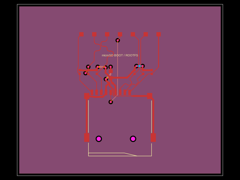 More from this authorShiboSoftwareDev/t113-s3-linux-computer-p9The code defines a PCB subcircuit for a buck converter module featuring a TMI3112H IC, FTC252010S power switch, and associated passive components like capacitors and resistors for voltage regulation and feedback control.
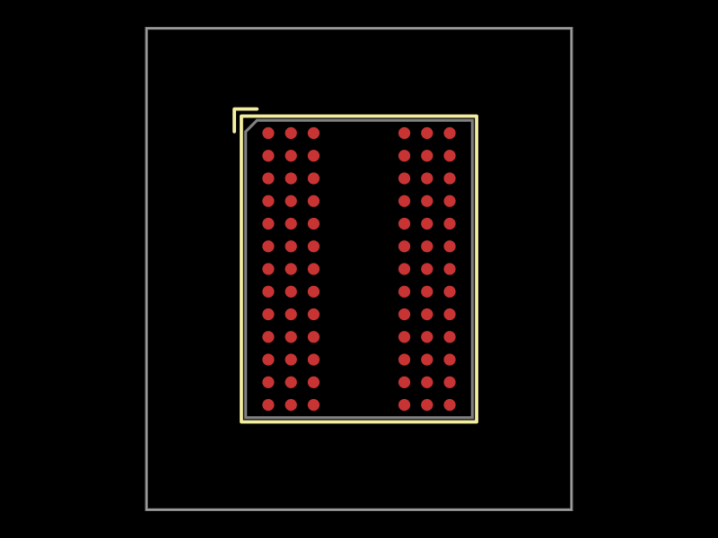 Similar package0hmX/mt41k512m8da-107-it-p-footprintsThis code defines the mechanical and physical layout of a Micron digital ball grid array (FBGA) package with 78 balls, including pin positions, footprint geometry, PCB pads, and silkscreen outlines for surface-mount integration.
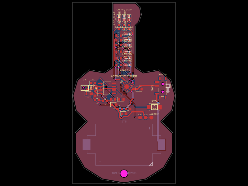 Discover something newgokul/acoustic-guitar-tunerThis code defines a miniature circuit board featuring a microcontroller (ATTINY1616-MNR), audio and power components, tactile switch, various LEDs, and passive components arranged with specific footprints, connections, and mechanical markings for a mini acoustic guitar tuner.