MustafaMulla29/wireless-mouse-pcb
This code defines a 3.3V low dropout voltage regulator chip (AP2112K-3.3TRG1) with five pins (VIN, GND, Enable, NC, VOUT) and its associated PCB footprint and 3D models for hardware implementation.
- Version
- 1.0.6
- License
- unset
- Stars
- 0
sections/WirelessControllerSection.tsx
import { A_2450AT18A100E } from "../imports/A_2450AT18A100E";
import { EVQPUC02K } from "../imports/EVQPUC02K";
import { NRF52810_QFAA_R } from "../imports/NRF52810_QFAA_R";
import { SDCL1005C3N9STDF } from "../imports/SDCL1005C3N9STDF";
import { S47SMD32_000M10PF10R30B3 } from "../imports/S47SMD32_000M10PF10R30B3";
import { NetTrace, POWER_TRACE, withSchematicSheet } from "./shared";

const BleSoc = NRF52810_QFAA_R as any;
const BleAntenna = A_2450AT18A100E as any;
const HfCrystal = S47SMD32_000M10PF10R30B3 as any;
const RfInductor3n9 = SDCL1005C3N9STDF as any;
const TactSwitch = EVQPUC02K as any;

// nRF52810-QFAA pin names and application-specific GPIO assignments.
// The peripheral signals can be mapped to these GPIOs in firmware.
const mcuPinLabels = {
  pin1: ["DEC1"],
  pin2: ["P0_00", "LFCLK_XL1", "DPI_BUTTON"],
  pin3: ["P0_01", "LFCLK_XL2"],
  pin4: ["P0_02", "AIN0", "ADC_VBAT"],
  pin5: ["P0_03", "MIDDLE_CLICK"],
  pin6: ["P0_04"],
  pin7: ["P0_05", "ENC_B"],
  pin8: ["P0_06"],
  pin9: ["P0_07", "ENC_A"],
  pin10: ["P0_08", "RIGHT_CLICK"],
  pin11: ["P0_09"],
  pin12: ["P0_10", "SENSOR_RESET"],
  pin13: ["VDD1"],
  pin14: ["P0_11"],
  pin15: ["P0_12", "SPI_SCLK"],
  pin16: ["P0_13"],
  pin17: ["P0_14", "SPI_MOSI"],
  pin18: ["P0_15", "SPI_MISO"],
  pin19: ["P0_16", "SENSOR_CS"],
  pin20: ["P0_17", "SENSOR_MOTION"],
  pin21: ["P0_18", "LEFT_CLICK"],
  pin22: ["P0_19"],
  pin23: ["P0_20"],
  pin24: ["P0_21", "RESET"],
  pin25: ["SWDCLK"],
  pin26: ["SWDIO"],
  pin27: ["P0_22"],
  pin28: ["P0_23"],
  pin29: ["P0_24"],
  pin30: ["ANT"],
  pin31: ["VSS_RF"],
  pin32: ["DEC2"],
  pin33: ["DEC3"],
  pin34: ["XC1"],
  pin35: ["XC2"],
  pin36: ["VDD3"],
  pin37: ["P0_25", "WLED_DATA"],
  pin38: ["P0_26"],
  pin39: ["P0_27", "SIDE1_BUTTON"],
  pin40: ["P0_28", "AIN4"],
  pin41: ["P0_29", "AIN5", "SIDE2_BUTTON"],
  pin42: ["P0_30", "AIN6"],
  pin43: ["P0_31", "AIN7"],
  pin44: ["NC"],
  pin45: ["VSS1"],
  pin46: ["DEC4"],
  pin47: ["DCC"],
  pin48: ["VDD2"],
  pin49: ["EP"],
} as const;

const unusedMcuPins = [
  "P0_04",
  "P0_06",
  "P0_09",
  "P0_11",
  "P0_13",
  "P0_22",
  "P0_23",
  "P0_24",
  "P0_26",
  "P0_28",
  "P0_20",
  "P0_30",
  "P0_31",
  "P0_01",
  "P0_19",
  "DEC2",
  "DCC",
  "NC",
];

export const WirelessControllerSection = () =>
  withSchematicSheet(
    "controller",
    <>
      <BleSoc
        name="U_MCU"
        pinLabels={mcuPinLabels}
        noConnect={unusedMcuPins}
        pinAttributes={{
          VDD1: { requiresPower: true },
          VDD2: { requiresPower: true },
          VDD3: { requiresPower: true },
          VSS_RF: { requiresGround: true },
          VSS1: { requiresGround: true },
          EP: { requiresGround: true },
          NC: { doNotConnect: true },
        }}
        schPinArrangement={{
          leftSide: {
            pins: [
              "VDD1",
              "VDD2",
              "VDD3",
              "VSS_RF",
              "VSS1",
              "EP",
              "DEC1",
              "DEC3",
              "DEC4",
              "LFCLK_XL1",
              "LFCLK_XL2",
              "XC1",
              "XC2",
              "ANT",
              "RESET",
              "ADC_VBAT",
            ],
            direction: "top-to-bottom",
          },
          rightSide: {
            pins: [
              "SPI_SCLK",
              "SPI_MOSI",
              "SPI_MISO",
              "SENSOR_CS",
              "SENSOR_MOTION",
              "SENSOR_RESET",
              "ENC_A",
              "ENC_B",
              "LEFT_CLICK",
              "RIGHT_CLICK",
              "MIDDLE_CLICK",
              "DPI_BUTTON",
              "SIDE1_BUTTON",
              "SIDE2_BUTTON",
              "WLED_DATA",
              "SWDIO",
              "SWDCLK",
            ],
            direction: "top-to-bottom",
          },
        }}
        schWidth={2.34}
        schHeight={3.4}
        pcbX={8}
        pcbY={22.5}
        pcbRotation={0}
        schX={-3}
        schY={0}
        schSectionName="WirelessController"
      />

      {/* Nordic nRF52810-QFAA internal-LDO reference decoupling. */}
      <capacitor
        name="C_MCU_VDD1"
        capacitance="100nF"
        footprint="0402"
        pcbX={13}
        pcbY={18}
        schX={-12}
        schY={6.4}
        schOrientation="vertical"
        schSectionName="WirelessController"
      />
      <capacitor
        name="C_MCU_VDD3"
        capacitance="100nF"
        footprint="0402"
        pcbX={3.2}
        pcbY={25.5}
        pcbRotation={180}
        schX={-10}
        schY={6.4}
        schOrientation="vertical"
        schSectionName="WirelessController"
      />
      <capacitor
        name="C_MCU_VDD2"
        capacitance="4.7uF"
        footprint="0603"
        pcbX={1.8}
        pcbY={20.3}
        pcbRotation={180}
        schX={-8}
        schY={6.4}
        schOrientation="vertical"
        schSectionName="WirelessController"
      />
      <capacitor
        name="C_MCU_DEC1"
        capacitance="100nF"
        footprint="0402"
        pcbX={5.8}
        pcbY={17.5}
        pcbRotation={270}
        schX={-6}
        schY={6.4}
        schOrientation="vertical"
        schSectionName="WirelessController"
      />
      <capacitor
        name="C_MCU_DEC3"
        capacitance="100pF"
        footprint="0402"
        pcbX={7.4}
        pcbY={27.2}
        pcbRotation={90}
        schX={-4}
        schY={6.4}
        schOrientation="vertical"
        schSectionName="WirelessController"
        supplierPartNumbers={{ jlcpcb: ["C1546"] }}
      />
      <capacitor
        name="C_MCU_DEC4"
        capacitance="1uF"
        footprint="0603"
        pcbX={3.2}
        pcbY={23}
        pcbRotation={270}
        schX={-2}
        schY={6.4}
        schOrientation="vertical"
        schSectionName="WirelessController"
      />

      {/* Mandatory 32 MHz radio clock. The firmware uses the calibrated LFRC. */}
      <HfCrystal
        name="X_HF_32M"
        pcbX={4}
        pcbY={32.6}
        pcbRotation={0}
        schX={-7}
        schY={-6.5}
        schWidth={1.2}
        schHeight={0.4}
        schSectionName="WirelessController"
      />
      <capacitor
        name="C_HF_XC1"
        capacitance="16pF"
        footprint="0402"
        pcbX={6.8}
        pcbY={29.3}
        pcbRotation={90}
        schX={-5.5}
        schY={-8}
        schOrientation="vertical"
        schSectionName="WirelessController"
        supplierPartNumbers={{ jlcpcb: ["C48836"] }}
      />
      <capacitor
        name="C_HF_XC2"
        capacitance="16pF"
        footprint="0402"
        pcbX={3.2}
        pcbY={29.3}
        pcbRotation={270}
        schX={-8.5}
        schY={-8}
        schOrientation="vertical"
        schSectionName="WirelessController"
        supplierPartNumbers={{ jlcpcb: ["C48836"] }}
      />

      <capacitor
        name="C_RESET"
        capacitance="100nF"
        footprint="0402"
        pcbX={15.5}
        pcbY={25}
        pcbRotation={90}
        schX={9}
        schY={6}
        schOrientation="vertical"
        schSectionName="StatusDebug"
      />
      <TactSwitch
        name="SW_RESET"
        noConnect={["pin3", "pin4"]}
        pcbX={-13}
        pcbY={31}
        pcbRotation={90}
        schX={12}
        schY={6.58}
        schSectionName="StatusDebug"
      />

      <NetTrace from=".U_MCU > .VDD1" to="net.V3V3" width={POWER_TRACE} />
      <NetTrace from=".U_MCU > .VDD2" to="net.V3V3" width={POWER_TRACE} />
      <NetTrace from=".U_MCU > .VDD3" to="net.V3V3" width={POWER_TRACE} />
      <NetTrace from=".U_MCU > .VSS_RF" to="net.GND" width={POWER_TRACE} />
      <NetTrace from=".U_MCU > .VSS1" to="net.GND" width={POWER_TRACE} />
      <NetTrace from=".U_MCU > .EP" to="net.GND" width={POWER_TRACE} />

      <NetTrace from=".C_MCU_VDD1 > .pin1" to="net.V3V3" width={POWER_TRACE} />
      <NetTrace from=".C_MCU_VDD1 > .pin2" to="net.GND" width={POWER_TRACE} />
      <NetTrace from=".C_MCU_VDD3 > .pin1" to="net.V3V3" width={POWER_TRACE} />
      <NetTrace from=".C_MCU_VDD3 > .pin2" to="net.GND" width={POWER_TRACE} />
      <NetTrace from=".C_MCU_VDD2 > .pin1" to="net.V3V3" width={POWER_TRACE} />
      <NetTrace from=".C_MCU_VDD2 > .pin2" to="net.GND" width={POWER_TRACE} />
      <NetTrace from=".U_MCU > .DEC1" to="net.DEC1" />
      <NetTrace from=".C_MCU_DEC1 > .pin1" to="net.DEC1" />
      <NetTrace from=".C_MCU_DEC1 > .pin2" to="net.GND" />
      <NetTrace from=".U_MCU > .DEC3" to="net.DEC3" />
      <NetTrace from=".C_MCU_DEC3 > .pin1" to="net.DEC3" />
      <NetTrace from=".C_MCU_DEC3 > .pin2" to="net.GND" />
      <NetTrace from=".U_MCU > .DEC4" to="net.DEC4" />
      <NetTrace from=".C_MCU_DEC4 > .pin1" to="net.DEC4" />
      <NetTrace from=".C_MCU_DEC4 > .pin2" to="net.GND" />

      <NetTrace from=".U_MCU > .XC1" to="net.XC1" />
      <NetTrace from=".X_HF_32M > .OSC2" to="net.XC1" />
      <NetTrace from=".C_HF_XC1 > .pin1" to="net.XC1" />
      <NetTrace from=".U_MCU > .XC2" to="net.XC2" />
      <NetTrace from=".X_HF_32M > .OSC1" to="net.XC2" />
      <NetTrace from=".C_HF_XC2 > .pin1" to="net.XC2" />
      <NetTrace from=".C_HF_XC1 > .pin2" to="net.GND" />
      <NetTrace from=".C_HF_XC2 > .pin2" to="net.GND" />

      <NetTrace from=".U_MCU > .RESET" to="net.RESET_N" />
      <NetTrace from=".C_RESET > .pin1" to="net.RESET_N" />
      <NetTrace from=".C_RESET > .pin2" to="net.GND" />
      <NetTrace from=".SW_RESET > .pin1" to="net.RESET_N" />
      <NetTrace from=".SW_RESET > .pin2" to="net.GND" />

      <NetTrace from=".U_MCU > .SPI_SCLK" to="net.SCLK" />
      <NetTrace from=".U_MCU > .SPI_MISO" to="net.MISO" />
      <NetTrace from=".U_MCU > .SPI_MOSI" to="net.MOSI" />
      <NetTrace from=".U_MCU > .SENSOR_CS" to="net.CS_N" />
      <NetTrace from=".U_MCU > .SENSOR_MOTION" to="net.MOTION" />
      <NetTrace from=".U_MCU > .SENSOR_RESET" to="net.S_RST" />
      <NetTrace from=".U_MCU > .ENC_A" to="net.ENC_A" />
      <NetTrace from=".U_MCU > .ENC_B" to="net.ENC_B" />
      <NetTrace from=".U_MCU > .LEFT_CLICK" to="net.LEFT" />
      <NetTrace from=".U_MCU > .RIGHT_CLICK" to="net.RIGHT" />
      <NetTrace from=".U_MCU > .MIDDLE_CLICK" to="net.MIDDLE" />
      <NetTrace from=".U_MCU > .DPI_BUTTON" to="net.DPI" />
      <NetTrace from=".U_MCU > .SIDE1_BUTTON" to="net.SIDE1" />
      <NetTrace from=".U_MCU > .SIDE2_BUTTON" to="net.SIDE2" />
      <NetTrace from=".U_MCU > .WLED_DATA" to="net.WLED" />
      <NetTrace from=".U_MCU > .ADC_VBAT" to="net.VBAT_ADC" />

      {/* Nordic output match, then Johanson's reference antenna T match:
          1 pF series, 2.7 nH shunt to GND, and 3.9 nH series toward the antenna.
          Keep the RF path compact. These widths are NOT a verified 50-ohm stackup;
          antenna matching still needs measurement on the assembled prototype. */}
      <capacitor
        name="C_RF_SHUNT"
        capacitance="0.8pF"
        footprint="0402"
        pcbX={8.7}
        pcbY={27.4}
        pcbRotation={90}
        schX={1}
        schY={-7}
        schOrientation="vertical"
        schSectionName="RadioFrontEnd"
        supplierPartNumbers={{ jlcpcb: ["C88902"] }}
      />
      <RfInductor3n9
        name="L_NRF_MATCH"
        pcbX={10.6}
        pcbY={27.4}
        pcbRotation={0}
        schX={3}
        schY={-7}
        schSectionName="RadioFrontEnd"
      />
      <capacitor
        name="C_ANT_MATCH"
        capacitance="1pF"
        footprint="0402"
        pcbX={11.15}
        pcbY={29.1}
        pcbRotation={0}
        schX={6}
        schY={-7}
        schOrientation="vertical"
        schSectionName="RadioFrontEnd"
        supplierPartNumbers={{ jlcpcb: ["C1550"] }}
      />
      <inductor
        name="L_ANT_SHUNT"
        inductance="2.7nH"
        footprint="0402"
        pcbX={13.1}
        pcbY={27.5}
        pcbRotation={270}
        schX={9}
        schY={-9}
        schOrientation="vertical"
        schSectionName="RadioFrontEnd"
        supplierPartNumbers={{ jlcpcb: ["C27123"] }}
      />
      <inductor
        name="L_ANT_MATCH_OUT"
        inductance="3.9nH"
        footprint="0402"
        pcbX={13.35}
        pcbY={29.1}
        pcbRotation={0}
        schX={12}
        schY={-7}
        schSectionName="RadioFrontEnd"
        supplierPartNumbers={{ jlcpcb: ["C14033"] }}
      />
      <BleAntenna
        name="ANT_BLE"
        noConnect={["pin2"]}
        pcbX={16.8}
        pcbY={29.1}
        pcbRotation={0}
        schX={15}
        schY={-7}
        schSectionName="RadioFrontEnd"
      />

      <NetTrace
        name="RF_OUT"
        from=".U_MCU > .ANT"
        to=".L_NRF_MATCH > .pin1"
        width="0.2mm"
      />
      <NetTrace
        name="RF_SHUNT"
        from=".L_NRF_MATCH > .pin1"
        to=".C_RF_SHUNT > .pin1"
        width="0.2mm"
      />
      <NetTrace from=".C_RF_SHUNT > .pin2" to="net.GND" width={POWER_TRACE} />
      <NetTrace
        name="RF1"
        from=".L_NRF_MATCH > .pin2"
        to=".C_ANT_MATCH > .pin1"
        width="0.5mm"
      />
      <NetTrace
        name="RF2"
        from=".C_ANT_MATCH > .pin2"
        to=".L_ANT_MATCH_OUT > .pin1"
        width="0.3mm"
      />
      <NetTrace
        name="RF_MATCH"
        from=".C_ANT_MATCH > .pin2"
        to=".L_ANT_SHUNT > .pin1"
        width="0.3mm"
      />
      <NetTrace from=".L_ANT_SHUNT > .pin2" to="net.GND" width={POWER_TRACE} />
      <NetTrace
        name="ANT_FEED"
        from=".L_ANT_MATCH_OUT > .pin2"
        to=".ANT_BLE > .ANT"
        width="0.3mm"
      />
    </>,
  );
Related Packages
 More from this authorMustafaMulla29/MSPM0G3507-tsxThe code defines a 64-pin QFP package of the Texas Instruments MSPM0G3507 ARM Cortex-M0+ microcontroller, detailing its pinout, electrical connections, and external support components such as decoupling capacitors, resistors, and headers for power management, debugging, and I/O functions.
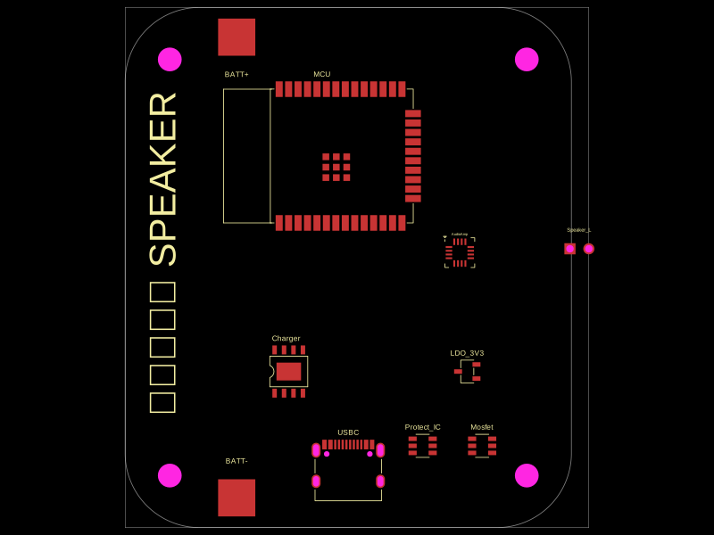 Similar packagemohan-bee/speakerThis code defines configurable 3D models and PCB footprints for various electronic components, including a battery charger IC, a dual Hall sensor, a dual power switch, and a voltage regulator, with detailed pinouts, footprints, and CAD models for schematic and physical design.
 Discover something newrushabhcodes/ESP32-E-ReaderThis code defines the physical layout and schematic wiring of an ESP32-based e-reader device, including various surface-mount components such as connectors, ICs, resistors, capacitors, inductors, diodes, pushbuttons, and an antenna, with precise PCB placement and interconnection details.