MustafaMulla29/wireless-mouse-pcb
This code defines a 3.3V low dropout voltage regulator chip (AP2112K-3.3TRG1) with five pins (VIN, GND, Enable, NC, VOUT) and its associated PCB footprint and 3D models for hardware implementation.
- Version
- 1.0.6
- License
- unset
- Stars
- 0
sections/UsbChargingSection.tsx
import { MCP73831T_2ACI_OT } from "../imports/MCP73831T_2ACI_OT";
import { TYPE_C_6P } from "../imports/TYPE_C_6P";
import { USBLC6_2SC6 } from "../imports/USBLC6_2SC6";
import { NetTrace, POWER_TRACE, withSchematicSheet } from "./shared";

const UsbCPart = TYPE_C_6P as any;

const usbCPinLabels = {
  pin7: ["SHELL1"],
  pin8: ["SHELL2"],
  pin9: ["SHELL3"],
  pin10: ["SHELL4"],
  pin11: ["GND1"],
  pin12: ["VBUS1"],
  pin13: ["CC1"],
  pin14: ["CC2"],
  pin15: ["VBUS2"],
  pin16: ["GND2"],
} as const;

export const UsbChargingSection = () =>
  withSchematicSheet(
    "power",
    <>
      <UsbCPart
        name="J_USB"
        pinLabels={usbCPinLabels}
        internallyConnectedPins={[
          ["GND1", "GND2"],
          ["SHELL1", "SHELL2", "SHELL3", "SHELL4"],
        ]}
        pcbX={0}
        pcbY={-29.7}
        pcbRotation={0}
        schX={-54.5}
        schY={0}
        schWidth={2.1}
        schHeight={1.2}
        schPinArrangement={{
          leftSide: {
            pins: ["SHELL1", "SHELL2", "GND1", "VBUS1", "CC1"],
            direction: "top-to-bottom",
          },
          rightSide: {
            pins: ["CC2", "VBUS2", "GND2", "SHELL3", "SHELL4"],
            direction: "top-to-bottom",
          },
        }}
        schSectionName="UsbCharging"
      />
      <USBLC6_2SC6
        name="U_USB_ESD"
        symbol={undefined}
        noConnect={["pin4", "pin6"]}
        pcbX={0}
        pcbY={-23.5}
        schX={-49}
        schY={-4}
        schWidth={1.8}
        schHeight={0.8}
        schPinArrangement={{
          leftSide: {
            pins: ["pin1", "pin2", "pin3"],
            direction: "top-to-bottom",
          },
          rightSide: {
            pins: ["pin6", "pin5", "pin4"],
            direction: "top-to-bottom",
          },
        }}
        schSectionName="UsbCharging"
      />
      <resistor
        name="R_CC1"
        resistance="5.1k"
        footprint="0402"
        pcbX={-6.5}
        pcbY={-32.5}
        schX={-50}
        schY={3}
        schSectionName="UsbCharging"
      />
      <resistor
        name="R_CC2"
        resistance="5.1k"
        footprint="0402"
        pcbX={6.5}
        pcbY={-32.5}
        schX={-47}
        schY={3}
        schSectionName="UsbCharging"
      />
      <capacitor
        name="C_USB_IN"
        capacitance="4.7uF"
        footprint="0805"
        pcbX={-4}
        pcbY={-23.5}
        pcbRotation={90}
        schX={-44}
        schY={3}
        schOrientation="vertical"
        schSectionName="UsbCharging"
      />
      <capacitor
        name="C_USB_IN_HF"
        capacitance="100nF"
        footprint="0603"
        pcbX={4.5}
        pcbY={-25.5}
        pcbRotation={90}
        schX={-44}
        schY={0.2}
        schOrientation="vertical"
        schSectionName="UsbCharging"
      />

      <MCP73831T_2ACI_OT
        name="U_CHARGER"
        pcbX={8}
        pcbY={-24}
        schX={-39}
        schY={0}
        schWidth={1.96}
        schHeight={0.6}
        schPinArrangement={{
          leftSide: {
            pins: ["VDD", "VSS", "PROG"],
            direction: "top-to-bottom",
          },
          rightSide: { pins: ["VBAT", "STAT"], direction: "top-to-bottom" },
        }}
        schSectionName="UsbCharging"
      />
      <resistor
        name="R_CHARGE_PROG"
        resistance="4.02k"
        footprint="0603"
        pcbX={13.6}
        pcbY={-27}
        schX={-39}
        schY={-4}
        schSectionName="UsbCharging"
      />
      <capacitor
        name="C_CHARGE_BAT"
        capacitance="4.7uF"
        footprint="0805"
        pcbX={10.8}
        pcbY={-27.2}
        pcbRotation={270}
        schX={-34}
        schY={-3}
        schOrientation="vertical"
        schSectionName="UsbCharging"
      />
      <resistor
        name="R_CHARGE_LED"
        resistance="1k"
        footprint="0603"
        pcbX={12}
        pcbY={-31}
        schX={-35.04}
        schY={3}
        schSectionName="UsbCharging"
      />
      <led
        name="LED_CHARGE"
        color="red"
        footprint="0603"
        supplierPartNumbers={{ jlcpcb: ["C965799"] }}
        pinLabels={{ pin1: ["cathode", "neg"], pin2: ["anode", "pos"] }}
        pcbX={15}
        pcbY={-31}
        pcbRotation={180}
        schX={-30}
        schY={3}
        schRotation={180}
        schSectionName="UsbCharging"
      />

      <NetTrace from=".J_USB > .VBUS1" to="net.VBUS" width={POWER_TRACE} />
      <NetTrace
        name="VBUS_LINK"
        from=".J_USB > .VBUS2"
        to=".J_USB > .VBUS1"
        width={POWER_TRACE}
      />
      <NetTrace from=".J_USB > .GND1" to="net.GND" width={POWER_TRACE} />
      <NetTrace from=".J_USB > .SHELL1" to="net.GND" width={POWER_TRACE} />

      <NetTrace from=".J_USB > .CC1" to="net.CC1" />
      <NetTrace from="net.CC1" to=".R_CC1 > .pin1" />
      <NetTrace from="net.CC1" to=".U_USB_ESD > .pin1" />
      <NetTrace from=".R_CC1 > .pin2" to="net.GND" />
      <NetTrace from=".J_USB > .CC2" to="net.CC2" />
      <NetTrace from="net.CC2" to=".R_CC2 > .pin1" />
      <NetTrace from="net.CC2" to=".U_USB_ESD > .pin3" />
      <NetTrace from=".R_CC2 > .pin2" to="net.GND" />
      <NetTrace from=".U_USB_ESD > .pin2" to="net.GND" />
      <NetTrace from=".U_USB_ESD > .pin5" to="net.VBUS" />

      <NetTrace from=".C_USB_IN > .pin1" to="net.VBUS" width={POWER_TRACE} />
      <NetTrace from=".C_USB_IN > .pin2" to="net.GND" width={POWER_TRACE} />
      <NetTrace from=".C_USB_IN_HF > .pin1" to="net.VBUS" />
      <NetTrace from=".C_USB_IN_HF > .pin2" to="net.GND" />
      <NetTrace from=".U_CHARGER > .VDD" to="net.VBUS" width={POWER_TRACE} />
      <NetTrace from=".U_CHARGER > .VSS" to="net.GND" width={POWER_TRACE} />
      <NetTrace from=".U_CHARGER > .VBAT" to="net.VBAT" width={POWER_TRACE} />
      <NetTrace
        name="CHG_PROG"
        from=".U_CHARGER > .PROG"
        to=".R_CHARGE_PROG > .pin1"
      />
      <NetTrace from=".R_CHARGE_PROG > .pin2" to="net.GND" />
      <NetTrace
        from=".C_CHARGE_BAT > .pin1"
        to="net.VBAT"
        width={POWER_TRACE}
      />
      <NetTrace from=".C_CHARGE_BAT > .pin2" to="net.GND" width={POWER_TRACE} />
      <NetTrace from="net.VBUS" to=".R_CHARGE_LED > .pin1" />
      <NetTrace
        name="CHG_LED"
        from=".R_CHARGE_LED > .pin2"
        to=".LED_CHARGE > .anode"
      />
      <NetTrace
        name="CHG_STAT"
        from=".LED_CHARGE > .cathode"
        to=".U_CHARGER > .STAT"
      />
    </>,
    42.5,
    6.2,
  );
Related Packages
 More from this authorMustafaMulla29/MSPM0G3507-tsxThe code defines a 64-pin QFP package of the Texas Instruments MSPM0G3507 ARM Cortex-M0+ microcontroller, detailing its pinout, electrical connections, and external support components such as decoupling capacitors, resistors, and headers for power management, debugging, and I/O functions.
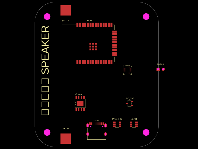 Similar packagemohan-bee/speakerThis code defines configurable 3D models and PCB footprints for various electronic components, including a battery charger IC, a dual Hall sensor, a dual power switch, and a voltage regulator, with detailed pinouts, footprints, and CAD models for schematic and physical design.
 Discover something newrushabhcodes/ESP32-E-ReaderThis code defines the physical layout and schematic wiring of an ESP32-based e-reader device, including various surface-mount components such as connectors, ICs, resistors, capacitors, inductors, diodes, pushbuttons, and an antenna, with precise PCB placement and interconnection details.