AnasSarkiz/ble-pedometer
This code defines and configures various electronic hardware components such as surface-mount resistors, crystals, diodes, transistors, connectors, and switches with their physical footprints, schematic symbols, and 3D CAD models for PCB assembly.
- Version
- 1.0.7
- License
- unset
- Stars
- 0
mcu-signal-fanout.tsx
import { Fragment } from "react"
import { pcbLayout } from "./pcb-layout"

// Stagger the north-side vias: 0.5 mm pin pitch is not enough for a straight
// row of 0.45 mm via pads. Offsets are in board axes from the MCU placement.
export const mcuSignalFanouts = [
  { name: "V_MCU_SCL", pin: "DIO24_A7", net: "I2C_SCL", x: -1.5, y: 2.95 },
  { name: "V_MCU_GAUGE_INT", pin: "DIO20_A11", net: "GAUGE_INT_N", x: 0.25, y: 2.95 },
  { name: "V_MCU_CHG_INT", pin: "DIO21_A10", net: "CHG_INT_N", x: -0.28, y: 2.45 },
  { name: "V_MCU_SDA", pin: "DIO12", net: "I2C_SDA", x: 3.25, y: 0.95 },
  { name: "V_MCU_PG", pin: "DIO6_A1", net: "CHG_PG_N", x: -1.6, y: -2.8 },
] as const

export const McuSignalFanout = () => <>
  {mcuSignalFanouts.map(({ name, pin, net, x, y }) => <Fragment key={name}>
    <via name={name} pcbX={pcbLayout.U1_MCU.pcbX + x} pcbY={pcbLayout.U1_MCU.pcbY + y}
      fromLayer="top" toLayer="bottom" holeDiameter="0.3mm" outerDiameter="0.45mm"
      connectsTo={`net.${net}`} />
    <trace name={`${name}_escape`} from={`.U1_MCU > .${pin}`} to={`.${name} > .bottom`}
      width="0.127mm" pcbPath={[`.${name} > .bottom`]} />
  </Fragment>)}
</>
Related Packages
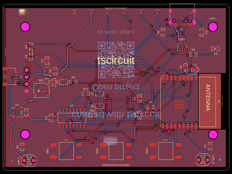 More from this authorAnasSarkiz/BlinkBuddyThis code defines and renders a 24mm square PCB silkscreen with a centered QR code graphic and labeling for open project instructions.
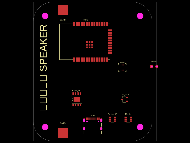 Similar packagemohan-bee/speakerThis code defines configurable 3D models and PCB footprints for various electronic components, including a battery charger IC, a dual Hall sensor, a dual power switch, and a voltage regulator, with detailed pinouts, footprints, and CAD models for schematic and physical design.
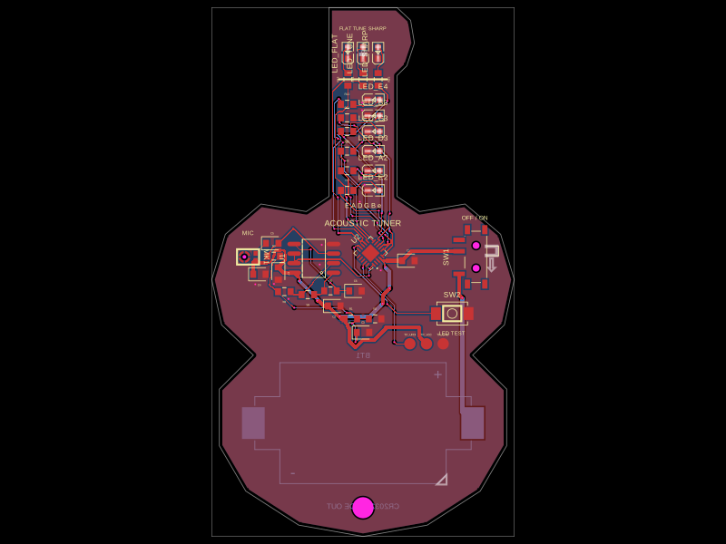 Discover something newgokul/acoustic-guitar-tunerThis code defines a miniature circuit board featuring a microcontroller (ATTINY1616-MNR), audio and power components, tactile switch, various LEDs, and passive components arranged with specific footprints, connections, and mechanical markings for a mini acoustic guitar tuner.