0hmX/mt41k512m8da-107-it-p-fanout
This code defines the physical footprint, routing, and layout configuration for a DDR3 memory module using surface-mount pads, vias, and copper traces on a printed circuit board (PCB).
- Version
- 0.2.3
- License
- unset
- Stars
- 0
tests/two-instances.circuit.tsx
import { MT41K512M8Fanout } from '../src/index'
export default () => <board width={45} height={30} layers={4} minTraceWidth={.12} minViaPadDiameter={.45} minViaHoleDiameter={.2}>
<MT41K512M8Fanout name="RAM0" pcbX={-10} pcbY={0} schX={-20} layoutProfile="outward_north" connections={{DQ0:"J1.pin1",ODT:"J2.pin1"}}/>
<MT41K512M8Fanout name="RAM1" pcbX={10} pcbY={0} pcbRotation={90} schX={20} layoutProfile="inward_south"/>
<pinheader name="J1" pinCount={1} pitch="2.54mm" footprint="pinrow1" pcbX={-20} pcbY={4.399992} schX={-20} schY={15}/>
<pinheader name="J2" pinCount={1} pitch="2.54mm" footprint="pinrow1" pcbX={-20} pcbY={0} schX={-15} schY={15}/>
</board>
Related Packages
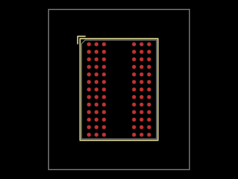 More from this author0hmX/mt41k512m8da-107-it-p-footprintsThis code defines the mechanical and physical layout of a Micron digital ball grid array (FBGA) package with 78 balls, including pin positions, footprint geometry, PCB pads, and silkscreen outlines for surface-mount integration.
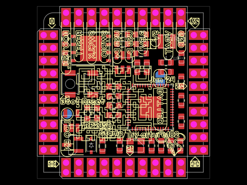 Similar packagetechmannih/imported-rp2350-stamp-boardThis code defines a detailed PCB layout with multiple layers, including the physical outline, component footprints, drilling holes, SMT pads, silkscreen markings, and courtyard outlines for component placement and board edges.
 Discover something newShiboSoftwareDev/mspm0g3507-usb-c-dev-boardThe circuit assembles a USB-C port with integrated ESD protection, power regulation, UART interface, and microcontroller (MSPM0G3507) with supporting components for USB data lines, CC termination, I2C, SPI, reset circuitry, and indicator LEDs.